Turn on suggestions
Auto-suggest helps you quickly narrow down your search results by suggesting possible matches as you type.
Showing results for
- STMicroelectronics Community
- STM32 MCUs
- STM32 MCUs Products
- Re: STM32F207 DMA PWM
Options
- Subscribe to RSS Feed
- Mark Topic as New
- Mark Topic as Read
- Float this Topic for Current User
- Bookmark
- Subscribe
- Mute
- Printer Friendly Page
STM32F207 DMA PWM
Options
- Mark as New
- Bookmark
- Subscribe
- Mute
- Subscribe to RSS Feed
- Permalink
- Email to a Friend
- Report Inappropriate Content
2016-11-24 01:06 PM
Posted on November 24, 2016 at 22:06 Chanel0...PWM output Chanel2... one of the GPIO bits controlled by the DMA Chanel3... toggle pin on CC1IF set Why is DMA transfer triggered on the Update and not on the Compare event? What am I doing wrong? Thanks! #stm32f2-dma-pwm
Hi,
I'm using STM32F207 and I would like to trigger DMA transfer on the falling edge of the PWM (duty cycle). So, I have configured TIM1 in PWM mode and enabled CC1DE and CCDS bits. uint8_t outBuffer[16] = {0}; int main(void) { RCC_ClocksTypeDef clocks; RCC_GetClocksFreq(&clocks); RCC_AHB1PeriphClockCmd(RCC_AHB1Periph_GPIOE, ENABLE); GPIO_InitTypeDef gpioStruct; GPIO_StructInit(&gpioStruct); gpioStruct.GPIO_Mode = GPIO_Mode_OUT; gpioStruct.GPIO_Pin = GPIO_Pin_All; gpioStruct.GPIO_OType = GPIO_OType_PP; gpioStruct.GPIO_PuPd = GPIO_PuPd_NOPULL; gpioStruct.GPIO_Speed = GPIO_Speed_100MHz; GPIO_Init(GPIOE, &gpioStruct); gpioStruct.GPIO_Pin = GPIO_Pin_9; gpioStruct.GPIO_Mode = GPIO_Mode_AF; gpioStruct.GPIO_OType = GPIO_OType_PP; gpioStruct.GPIO_PuPd = GPIO_PuPd_NOPULL; gpioStruct.GPIO_Speed = GPIO_Speed_50MHz; GPIO_Init(GPIOE, &gpioStruct); /* Connect TIM1 pins to AF */ GPIO_PinAFConfig(GPIOE, GPIO_PinSource9, GPIO_AF_TIM1); for (uint32_t i = 0; i < 15; i+=2) { outBuffer[i] = 0xAAAA; outBuffer[i+1] = ~0xAAAA; } TIM1_Config(100000); DMA2_Config(); while(1) { if(TIM_GetFlagStatus(TIM1, TIM_FLAG_CC1) == SET) { GPIO_ToggleBits(GPIOE, GPIO_Pin_14); TIM_ClearFlag(TIM1, TIM_FLAG_CC1); } } } void DMA2_Config(void) { DMA_InitTypeDef DMAInitStruct; RCC_AHB1PeriphClockCmd(RCC_AHB1Periph_DMA2 , ENABLE); DMA_DeInit(DMA2_Stream1); DMAInitStruct.DMA_Channel = DMA_Channel_6; DMAInitStruct.DMA_PeripheralBaseAddr = (uint32_t)(GPIOE_BASE) + 0x14; DMAInitStruct.DMA_Memory0BaseAddr = (uint32_t)&outBuffer; DMAInitStruct.DMA_DIR = DMA_DIR_MemoryToPeripheral; DMAInitStruct.DMA_BufferSize = 16; DMAInitStruct.DMA_PeripheralInc = DMA_PeripheralInc_Disable; DMAInitStruct.DMA_MemoryInc = DMA_MemoryInc_Enable; DMAInitStruct.DMA_MemoryDataSize = DMA_MemoryDataSize_Byte; DMAInitStruct.DMA_PeripheralDataSize = DMA_PeripheralDataSize_Byte; DMAInitStruct.DMA_Mode = DMA_Mode_Circular; DMAInitStruct.DMA_Priority = DMA_Priority_High; DMAInitStruct.DMA_FIFOMode = DMA_FIFOMode_Disable; DMAInitStruct.DMA_FIFOThreshold = DMA_FIFOThreshold_HalfFull; DMAInitStruct.DMA_MemoryBurst = DMA_MemoryBurst_Single; DMAInitStruct.DMA_PeripheralBurst = DMA_PeripheralBurst_Single; DMA_Init(DMA2_Stream1, &DMAInitStruct); TIM_DMACmd(TIM1, TIM_DMA_CC1, ENABLE); DMA_Cmd(DMA2_Stream1, ENABLE); TIM_Cmd(TIM1, ENABLE); } But what I get is the DMA transfer triggerd on the Update event... Chanel0...PWM output Chanel2... one of the GPIO bits controlled by the DMA Chanel3... toggle pin on CC1IF set Why is DMA transfer triggered on the Update and not on the Compare event? What am I doing wrong? Thanks! #stm32f2-dma-pwm
Labels:
- Labels:
-
DMA
5 REPLIES 5
Options
- Mark as New
- Bookmark
- Subscribe
- Mute
- Subscribe to RSS Feed
- Permalink
- Email to a Friend
- Report Inappropriate Content
2016-11-24 04:08 PM
Posted on November 25, 2016 at 01:08
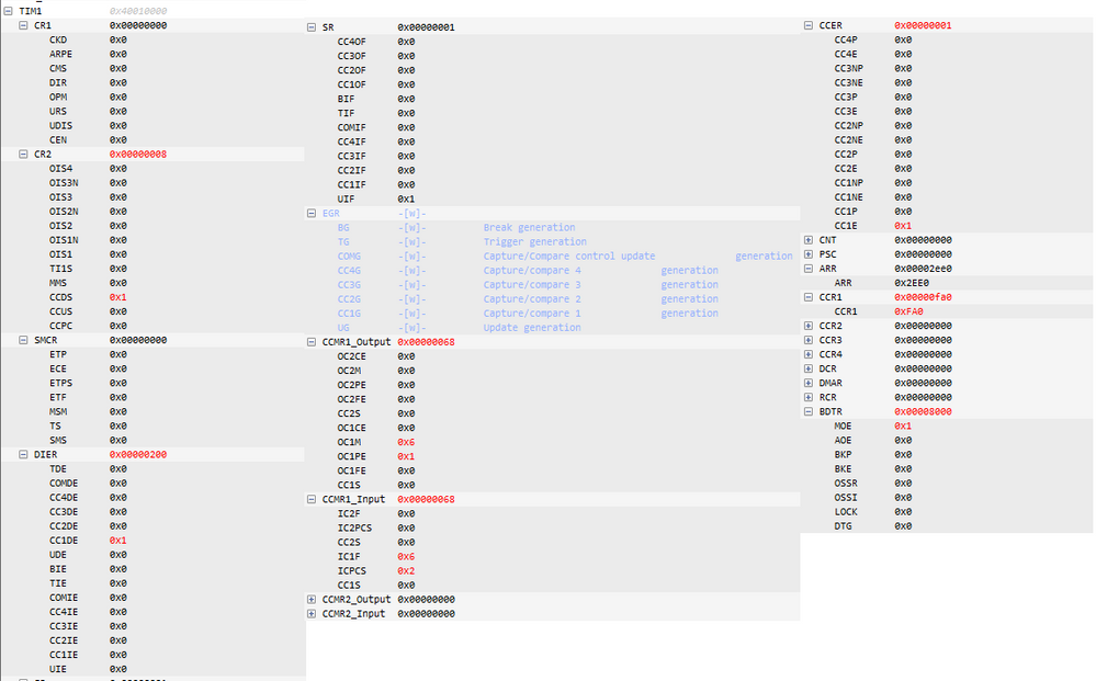
Post the content of timer registers.
JWOptions
- Mark as New
- Bookmark
- Subscribe
- Mute
- Subscribe to RSS Feed
- Permalink
- Email to a Friend
- Report Inappropriate Content
2016-11-28 10:17 AM
Posted on November 28, 2016 at 19:17
Sorry for the delay, I didn't have the board by my side for a few days...
Here is the content of the TIM1 registers right before enabling the timer
Options
- Mark as New
- Bookmark
- Subscribe
- Mute
- Subscribe to RSS Feed
- Permalink
- Email to a Friend
- Report Inappropriate Content
2016-11-28 11:30 AM
Posted on November 28, 2016 at 20:30
> CCDS 0x01
Don't. Bit 3 CCDS: Capture/compare DMA selection 0: CCx DMA request sent when CCx event occurs 1: CCx DMA requests sent when update event occurs JWOptions
- Mark as New
- Bookmark
- Subscribe
- Mute
- Subscribe to RSS Feed
- Permalink
- Email to a Friend
- Report Inappropriate Content
2016-11-28 11:33 AM
Posted on November 28, 2016 at 20:33
I see the source of your confusion.
17.3.9 Output compare modeWhen a match is found between the capture/compare register and the counter, the output
compare function:
[...]
Sends a DMA request if the corresponding enable bit is set (CCxDE bit in the
TIMx_DIER register, CCDS bit in the TIMx_CR2 register for the DMA request
selection).
Very badly formulated, but sadly it's no surprise. JW
Options
- Mark as New
- Bookmark
- Subscribe
- Mute
- Subscribe to RSS Feed
- Permalink
- Email to a Friend
- Report Inappropriate Content
2016-11-28 02:04 PM
Posted on November 28, 2016 at 23:04
excellent observation :)
thanks, it works now... btw CCDS basically excludes triggering DMA transfer on CC and Update which means that one can't trigger two different streams with one timer? For example if I would like to trigger two DMA transfers, one on the falling end and the other on the rising edge of a PWM (CC and Update) is it feasible with one timer? Doesn't look so...
Related Content
- ECC key decompression in X-CUBE-CRYPTOLIB in STM32 MCUs Security
- MQTT_VAR_HEADER_BUFFER_LEN in STM32CubeIDE (MCUs)
- UART loop in STM32H753 in STM32 MCUs Products
- Nucleo-STM32F207 LwIP TCP CLIENT fails to connect to the server in STM32CubeMX (MCUs)
- LWIP STM32, if ethernet cable not connected, tcp server not accepting client connection in STM32 MCUs Products