- STMicroelectronics Community
- STM32 MCUs
- STM32 MCUs Products
- Re: Pwm input mode F401RE
- Subscribe to RSS Feed
- Mark Topic as New
- Mark Topic as Read
- Float this Topic for Current User
- Bookmark
- Subscribe
- Mute
- Printer Friendly Page
Pwm input mode F401RE
- Mark as New
- Bookmark
- Subscribe
- Mute
- Subscribe to RSS Feed
- Permalink
- Email to a Friend
- Report Inappropriate Content
2017-10-30 3:09 AM
Hi, i have a problem about pwm input mode for f401re board. Forse my purpose, I use cubemx and set Tim 9 slave controller in reset mode, TI1FP1 ad trigger source, Channel 1 in input capture direct mode and Channel 2 in input capture indirect mode, as It is written in ref manual. Then I thick 'internal clock', choose an ARR value and prescaler values compatible with my test signal to mesure and generate the code.
On IAR, I only enable timer input capture mode using 'HAL_TIM_IC_Start(&htim9,TIM_CHANNEL_ALL' function. What i see is that the counter Tim 9 works, CNT is continuosly updated, but Tim9_ccr1 and tim9_ccr2 always remain at 0 values despite the test pwm signal has the right frequency according to counter's range. It seems the board doesn t recognize signal's edges. On reference manual is written that ccrx values should not reset despite of the reset mode. So, is there anything else to do?
Thanks for all the answer. Best regards.
#stm32-f4 #pwm #input-capture-mode Note: this post was migrated and contained many threaded conversations, some content may be missing.- Labels:
-
STM32F4 Series
-
TIM
- Mark as New
- Bookmark
- Subscribe
- Mute
- Subscribe to RSS Feed
- Permalink
- Email to a Friend
- Report Inappropriate Content
2017-10-30 3:15 AM
GPIO for given pin set properly?
Read out related GPIO and TIM registers' content and post.
JW
- Mark as New
- Bookmark
- Subscribe
- Mute
- Subscribe to RSS Feed
- Permalink
- Email to a Friend
- Report Inappropriate Content
2017-10-31 7:41 AM
Hi, thanks a lot for the answer.
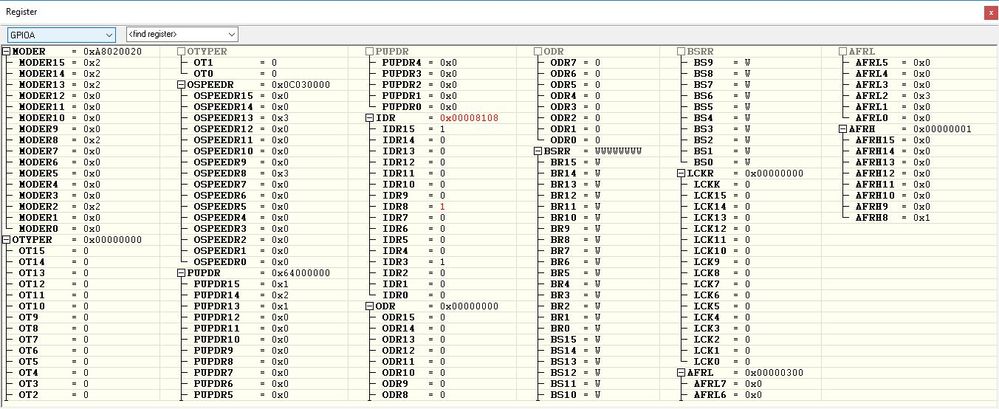
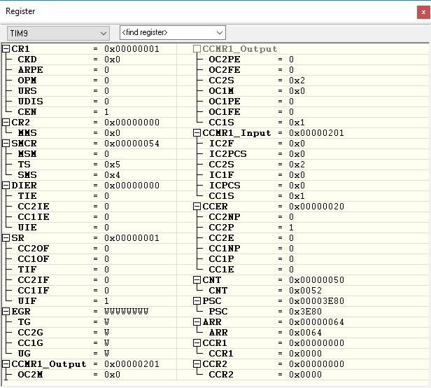
Here are posted screens about TIM9 and GPIOA.
In this particular project the same board generate also PWM signal, using another timer (TIM1). If I use two different board, the result is the same. PA2 is a pin linked to TIM9, used to acquire information from a PWM signal. PA8 is linked to TIM1 which generates PWM signal. It seems that the generation has success. Otherwise, IDR8 is costant, but it changes.

GPIOA

TIM9
I notice that CC2IE and CC1IE are at 0 value. I modify it manually but the result is the same.
- Mark as New
- Bookmark
- Subscribe
- Mute
- Subscribe to RSS Feed
- Permalink
- Email to a Friend
- Report Inappropriate Content
2017-10-31 7:49 AM
Neither channel's capture is enabled in CCER.
JW
- Mark as New
- Bookmark
- Subscribe
- Mute
- Subscribe to RSS Feed
- Permalink
- Email to a Friend
- Report Inappropriate Content
2017-10-31 8:30 AM
I enable it but nothing.
Should HAL function (HAL_TIM_IC_Start) set these registers automatically?
- Mark as New
- Bookmark
- Subscribe
- Mute
- Subscribe to RSS Feed
- Permalink
- Email to a Friend
- Report Inappropriate Content
2017-10-31 8:47 AM
I enable it but nothing.
Do you see GPIOA->IDR bit 2 to change in the debugger (in other words, are you sure there is valid input to PA2)?
You have set a relatively big prescaler on TIM9, are you sure the PWM input is slow enough?
If you don't set the reset mode (i.e. set TIM9_SMCR.SMS=0), do you see the values in TIM9_CCR1/CCR2 changing?
Should HAL function (HAL_TIM_IC_Start) set these registers automatically?
I don't and won't use Cube.
JW
- Mark as New
- Bookmark
- Subscribe
- Mute
- Subscribe to RSS Feed
- Permalink
- Email to a Friend
- Report Inappropriate Content
2017-10-31 9:19 AM
Do you see GPIOA->IDR bit 2 to change in the debugger (in other words, are you sure there is valid input to PA2)?
You have set a relatively big prescaler on TIM9, are you sure the PWM input is slow enough?
PWM signal is generated by TIM1 on the same board. The prescaler is the same and its ARR value is less then the TIM9's ARR value. However IDR2 doesn't change. I wired D1 (PA2) and D7 (PA8) which are input and output pins.
If you don't set the reset mode (i.e. set TIM9_SMCR.SMS=0), do you see the values in TIM9_CCR1/CCR2 changing?
No.
I don't and won't use Cube.
Maybe I should do it, too...
- Mark as New
- Bookmark
- Subscribe
- Mute
- Subscribe to RSS Feed
- Permalink
- Email to a Friend
- Report Inappropriate Content
2017-10-31 10:09 AM
Do you have an oscilloscope to check this, * directly * at the PA2 pin of the mcu? What board is this? Isn't there something else on PA2?
JW
- Mark as New
- Bookmark
- Subscribe
- Mute
- Subscribe to RSS Feed
- Permalink
- Email to a Friend
- Report Inappropriate Content
2017-11-01 5:42 AM
I use ADC on the board and there is the correct swing from VDD to GND and viceversa on PA2.
- Mark as New
- Bookmark
- Subscribe
- Mute
- Subscribe to RSS Feed
- Permalink
- Email to a Friend
- Report Inappropriate Content
2017-11-01 12:17 PM
That's more hummm.
PA2 is also TIM5_CH3. Can you please try to set it up in GPIO for AF2 for TIM5, set TIM5 to run (enable clock in RCC, ARR=0xFFFFFFFF, CR1.CEN=1), CH3 for straight capture (CCMR2.CC3S = 1, CCER.CC3E = 1) and observe CCR3?
JW
- STM32L5 Stop2 and Comparator in STM32 MCUs Products
- Incorrect ADC values when using HAL setup for DISCO-L475VG-IOT01A in STM32 MCUs Embedded software
- GPIO & EXTI: switching between input & output in STM32 MCUs Products
- Fail to load images from the SD card in STM32 MCUs TouchGFX and GUI
- SHCI_C2_FUS_LoadUsrKey doesn't load AES1 key registers in STM32 MCUs Security