- STMicroelectronics Community
- STM32 MCUs
- STM32 MCUs Products
- Re: NAND FLASH 25N01GV with STM32H725 sector erase...
- Subscribe to RSS Feed
- Mark Topic as New
- Mark Topic as Read
- Float this Topic for Current User
- Bookmark
- Subscribe
- Mute
- Printer Friendly Page
NAND FLASH 25N01GV with STM32H725 sector erase failure
- Mark as New
- Bookmark
- Subscribe
- Mute
- Subscribe to RSS Feed
- Permalink
- Email to a Friend
- Report Inappropriate Content
2023-11-19 11:50 PM
Hello everyone, I am trying to use STM32H725 processor with NAND FLASH 25N01GV. The installation seems successful. But sector erase always fails with the same error Status Register(0xC0) = 0x04 (EFAIL - Erase Failure )
1. JEDEC ID read successful.
W25XXX_OP_READ_JEDEC_ID
WRITE | DUMMY | READ |
0x9F | 1 BYTES | 0xEF,0xAA,0x21 |
2. Setting Up FLASH IC
a. W25XXX_OP_RST
WRITE | DUMMY | READ |
0xFF | 0 BYTES |
|
b. W25XXX_OP_WRITE_ENABLE
WRITE | DUMMY | READ |
0x06 | 0 BYTES |
|
c. READ W25XXX_REG_CONF (RD REGISTER 0xB0 = 0x18 )
WRITE | DUMMY | READ |
0x05,0xB0 | 0 BYTES | 0x18 (En ECC, Buffer Mode) |
d. WRITE W25XXX_REG_PROT (WR REGISTER 0xA0 = 0x00 )
WRITE | DUMMY | READ |
0x01,0xA0,0x00 | 0 BYTES |
|
e. WRITE W25XXX_REG_CONF (WR REGISTER 0xB0 = 0x18 )
WRITE | DUMMY | READ |
0x01,0xB0,0x18 | 0 BYTES |
|
e. READ W25XXX_OP_BBM_READ_LUT (RD LUTs 0xA5 = 0x00,0x00,.., 0x00 )
WRITE | DUMMY | READ |
0x0A5 | 1 BYTES | 0x00,0x00,.., 0x00 (80 bytes) |
f. READ W25XXX_OP_BBM_READ_LUT (RD LUTs 0xA5 = 0x00,0x00,.., 0x00 )
WRITE | DUMMY | READ |
0x0A5 | 1 BYTES | 0x00,0x00,.., 0x00 (80 bytes) |
3. Sector Erase:
a. WRITE W25XXX_OP_BLOCK_ERASE (BLOCK ERASE 0xD8 = 0x0000 )
WRITE | DUMMY | READ |
0xD8,0x00,0x00,0x00 | 1 BYTES |
|
b. READ W25XXX_REG_STAT (RD REGISTER 0xC0 = 0x04 )
WRITE | DUMMY | READ |
0x05,0xC0 | 0 BYTES | 0x04 (EFAIL - Erase Failure ) |
- Labels:
-
QSPI
-
STM32H7 Series
- Mark as New
- Bookmark
- Subscribe
- Mute
- Subscribe to RSS Feed
- Permalink
- Email to a Friend
- Report Inappropriate Content
2023-11-20 12:13 AM - edited 2023-11-20 12:30 AM
Hello @Ayaki.11 ,
This issue is already posted these discussion:
Solved: Re: STM32WB QSPI FLASH - Winbond(W25N01GV) - STMicroelectronics Community
Solved: Re: [STM32H750BX][QSPI] Issue with W25N01GVZEIG NA... - STMicroelectronics Community
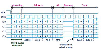
The memory is supported if the command format is in line with the OCTOSPI controller frame format (AN5050):
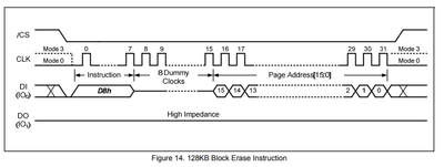
But, according to the memory datasheet, Block Erase (D8h) command needs the address after the dummy bytes.
Thank you.
Kaouthar
To give better visibility on the answered topics, please click on Accept as Solution on the reply which solved your issue or answered your question.
- Mark as New
- Bookmark
- Subscribe
- Mute
- Subscribe to RSS Feed
- Permalink
- Email to a Friend
- Report Inappropriate Content
2023-11-20 12:26 AM
Thank you for your answer. I know that it is necessary to send an 8-bit dummy after the SECTOR ERASE command. You can see this if you look at the end of the tables. I think the source of the problem I am experiencing is different.
3. Sector Erase:
a. WRITE W25XXX_OP_BLOCK_ERASE (BLOCK ERASE 0xD8 = 0x0000 )
WRITE | DUMMY | READ |
0xD8,0x00,0x00,0x00 | 1 BYTES |
|
- Mark as New
- Bookmark
- Subscribe
- Mute
- Subscribe to RSS Feed
- Permalink
- Email to a Friend
- Report Inappropriate Content
2023-11-20 02:02 AM
Hi @Ayaki.11 ,
To clarify my last comment, the microcontroller sends the OCTOSPI command fields in the following order:
- Instruction
- Address
- Alternate bytes
- Dummy
- Data
But, the erase command needs the address after the dummy bytes, not before. This command does not follow the order supported by OCTOSPI controller frame format.
Please take a look to this discussion.
Thank you.
Kaouthar
To give better visibility on the answered topics, please click on Accept as Solution on the reply which solved your issue or answered your question.
- Mark as New
- Bookmark
- Subscribe
- Mute
- Subscribe to RSS Feed
- Permalink
- Email to a Friend
- Report Inappropriate Content
2023-11-20 03:11 AM
Thanks again. I know that. Erase sector sequence is COMMAND+DUMMY BYTES+ADDRESS. But order is not important for my example. My Address= 0x0000 and I write dummy bytes as 0x00. My output data is 0xD8,0x00,0x00,0x00.
- Mark as New
- Bookmark
- Subscribe
- Mute
- Subscribe to RSS Feed
- Permalink
- Email to a Friend
- Report Inappropriate Content
2023-11-20 03:13 AM
I've used these but not spent much time with them.
Looks at Flight Controller BlackBox implementations. Review data sheet. Watch for block protection or alignment if erase fails. Form of address passed.
Up vote any posts that you find helpful, it shows what's working..
- Mark as New
- Bookmark
- Subscribe
- Mute
- Subscribe to RSS Feed
- Permalink
- Email to a Friend
- Report Inappropriate Content
2023-11-20 05:40 AM
Apparently I cannot write the correct value for Protection Register / Status Register-1 (0xA0 = 0x7C). I try to write 0x02 but operation can not be successfull.

