- STMicroelectronics Community
- STM32 MCUs
- STM32 MCUs Products
- Impact of end voltage on sampling capacitor on nex...
- Subscribe to RSS Feed
- Mark Topic as New
- Mark Topic as Read
- Float this Topic for Current User
- Bookmark
- Subscribe
- Mute
- Printer Friendly Page
Impact of end voltage on sampling capacitor on next conversion of high-impedance input
- Mark as New
- Bookmark
- Subscribe
- Mute
- Subscribe to RSS Feed
- Permalink
- Email to a Friend
- Report Inappropriate Content
2023-11-26 10:03 AM - edited 2023-11-26 10:07 AM
This is not description of normal ADC operation, but experiment aimed at revealing of details of the ADC internals, inspired by this thread.
I wrote a simple program for a 'F407-Disco (in attachment), which performs a 2-step sequence of ADC conversions, on PA3 and then on PA1. PA1 is floating, loaded only by impedance of scope probe (14pF, 10x1MOhm). PA3 is connected (using the jumpers provided conveniently with the Disco on its "legs" in the northern corners - nice touch, ST) with PA2 and PA0, and by setting those two pins to output-high, output-low, and combinations of pullups and pulldowns (there's also an external pulldown on PA0) provides four input levels onto PA3.
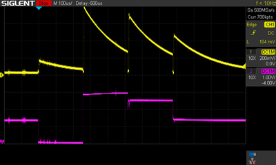
After "resetting" PA1 to zero (by setting it to output momentarily) and setting voltage on PA3, are two modes: a single ADC sequence followed by a delay, resulting in a peak and decay on PA1 (yellow CH1 - PA1, 200mV/div, purple CH2 - 1V/div)
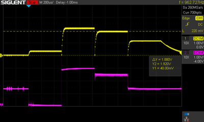
and repeated ADC sequences resulting in voltage on PA1 increasing to a certain steady level (yellow CH1 - PA1, 1V/div, purple CH2 - 1V/div):
Measured values:
Results:                  SINGLE CONVERSIONS      REPEATED CONVERSIONS
     PA3(+PA2+PA0)  PA1*   calc    raw data       PA1*   calc    raw data
(1)  0.00           0.15  {0.08}  {   0,  112}    0.30  {0.26}  {   4,  370}
{2}  2.90           0.78  {0.73}  {4095, 1024}    2.12  {2.14}  {4095, 3025}
(3)  2.50           0.68  {0.64}  {3511,  902}    1.88  {1.86}  {3421, 2631}
(4)  1.35           0.45  {0.40}  {1887,  563}    1.14  {1.11}  {1863, 1565}

* PA1 is measured voltage of the peak/steady state for single/repeated conversions
  calc is voltage calculated from the ADC conversion (i.e. 2.90V / 4095 * data[n][1])
  all voltages in [V]
*/
The "steady state" PA1 voltages for the repeated conversions experiment have a roughly linear dependence on the PA3 voltage:
PA1steady = 0.3V + 0.6 * PA3
I don't know how to interpret this result.
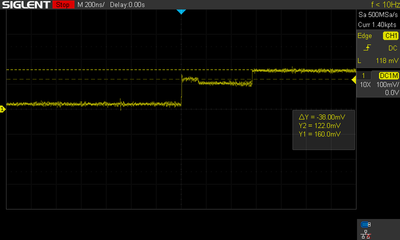
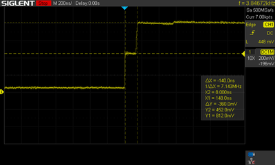
There are also some details which may or may not indicate that the underlying processes are somewhat more compliated. For example, with 0V on PA3, while the "single pulse" voltage achieved around 0.15V, the converted value was equivalent of cca half of that. Also, details on the "single pulse" conversion (200ns per div, ADC runs on default 16MHz HSI and default 3 cycle sampling, i.e. sampling duration is cca 188ns, conversion is 12 cycles i.e. 562ns) are interesting and suggest that part of the observed voltage increase happens at the beginning of the sampling cycle and part at the end (maybe half cycle before end?), with another voltage step at the end of conversion. First PA1 waveform is for PA3=0V, second is for PA3=VDD=2.9V:
Corollary is, that
- it's important to have a low enough impedance signal driving ADC input
- portion of voltage from previous conversion plus a DC offset remains on through the sampling capacitor to the next conversion, and that may impact next conversion if the signal impedance is high
- above findings are 'F407-specific; ADCs in STM32 vary significantly among families/models
JW
- Labels:
-
ADC
-
STM32F4 Series
- Mark as New
- Bookmark
- Subscribe
- Mute
- Subscribe to RSS Feed
- Permalink
- Email to a Friend
- Report Inappropriate Content
2023-11-26 11:20 AM - edited 2023-11-26 11:20 AM
On a local Czech/Slovak mailing list, I received a comment, that the difference between expected "previous conversion voltage" and the observed one can be explained to certain extent by charge injection through the switch(es). @TDK mentioned this,. too, in the "original" thread, and I guess that indeed might explain a lot (although thus the intimate details get even more complicated).
JW
- Mark as New
- Bookmark
- Subscribe
- Mute
- Subscribe to RSS Feed
- Permalink
- Email to a Friend
- Report Inappropriate Content
2023-11-26 12:14 PM
Dear @waclawek.jan ,
Thanks for the nice testing which is common to many SAR ADC and known as charge transfer from the sampling to the source . We detailed that behavior in our Application Note
Section 4.4 and then 4.4.4
Cheers,
STOne-32
- Mark as New
- Bookmark
- Subscribe
- Mute
- Subscribe to RSS Feed
- Permalink
- Email to a Friend
- Report Inappropriate Content
2023-11-26 05:45 PM
Thanks for testing and posting!
> it's important to have a low enough impedance signal driving ADC input
+1
The amount of people using the ADC on floating inputs and drawing conclusions from that is way too high.
- How to test real ADC frequency and its accuracy? in STM32 MCUs Products
- STM32G431KB ADC Wrong value in STM32 MCUs Products
- Recommended resistor and power ratings for STM32F105 ADC in STM32 MCUs Products
- What is the difference between Oversampling Continued vs Resumed mode in ADC? in STM32 MCUs Products
- STM32F429 Discovery multiple textArea update problem in STM32 MCUs TouchGFX and GUI


