- STMicroelectronics Community
- STM32 MCUs
- STM32 MCUs Products
- Re: How is the first byte transmitted in the SPI p...
- Subscribe to RSS Feed
- Mark Topic as New
- Mark Topic as Read
- Float this Topic for Current User
- Bookmark
- Subscribe
- Mute
- Printer Friendly Page
How is the first byte transmitted in the SPI protocol?
- Mark as New
- Bookmark
- Subscribe
- Mute
- Subscribe to RSS Feed
- Permalink
- Email to a Friend
- Report Inappropriate Content
2017-10-24 01:18 AM
Hi,
I'm new to embedded electronics, and have started learning by using the STM32F407VG discovery board. Overall, I think I understand the SPI protocol, but there are a few things that I'm not understanding fully with regards to data transmission.

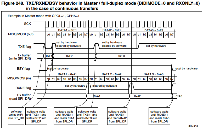
As per the graph above, the first byte (0xF1) is transmitted in the time of one bit (and one clock cycle). The other bytes (0xF2 and 0xF3) are transmitted into the TX buffer in the time of one byte. Why is this?
The RXNE flag is issued before the time of the eight bit in 0xF1, and is up only for a short period of time. Does all of the data RX'ing of the first bit happen in that short period of time?
There is something I'm not understanding clearly enough about the timing of these events. Please explain, and thank you in advance.
#spi #stm32f407 #rx #tx- Labels:
-
SPI
-
STM32F4 Series
- Mark as New
- Bookmark
- Subscribe
- Mute
- Subscribe to RSS Feed
- Permalink
- Email to a Friend
- Report Inappropriate Content
2017-10-24 01:34 AM
That's from the point of view of the program. The SPI is double-buffered, it means, there's a holding register (a 1-byte FIFO) and a shift register. When the SPI is idle, the first byte written by program to the holding register goes to shift register and starts to be shifted out bit-by-bit almost immediately, then the second goes to the holding register and has to wait until the first got shifted out from the shift register.
JW
- Mark as New
- Bookmark
- Subscribe
- Mute
- Subscribe to RSS Feed
- Permalink
- Email to a Friend
- Report Inappropriate Content
2017-10-24 04:25 AM
I see. So because the shift register is empty, in the time of one clock cycle, an entire byte of data enters the shift register. From there, the data is shifted out bit by bit to the RX holding register. But if that's the case, why is it that the RXNE flag is active before 8 clock cycles, and not after 9 clock cycles (1 clock cycle in TX'ing data to the shift register, and then 8 clock cycles in transferring to the RX holding register)?
- Mark as New
- Bookmark
- Subscribe
- Mute
- Subscribe to RSS Feed
- Permalink
- Email to a Friend
- Report Inappropriate Content
2017-10-24 04:37 AM
Rx and Tx shifts work on opposite SCK clock edges.
Why the TXE signal is delayed 1 bit after the actual transfer from holding to shift register, is given by the internal implementation of the SPI module.
JW
- Mark as New
- Bookmark
- Subscribe
- Mute
- Subscribe to RSS Feed
- Permalink
- Email to a Friend
- Report Inappropriate Content
2017-10-24 04:59 AM
I see so the transfer from the holding to shift register is more or less instantaneous (i.e. doesn't actually take one clock cycle)
- Mark as New
- Bookmark
- Subscribe
- Mute
- Subscribe to RSS Feed
- Permalink
- Email to a Friend
- Report Inappropriate Content
2017-10-24 05:14 AM
And the bits are loaded all at once from the holding register to the TX or RX buffer.
- Regarding the working of the code and few modifications as per needed in the generated code of motor control workbench in STM32 MCUs Products
- NUCLEO H723ZGT connect to BMI270 Mikroe via SPI in STM32 MCUs Boards and hardware tools
- I2C Slave device implementation ACK/NACK problem in STM32 MCUs Products
- How to use the WiFi on B-L4S5I-IOT01A ? in STM32 MCUs Boards and hardware tools
- Matter protocol Ethernet (LwIP?) Examples in STM32 MCUs Wireless