- Subscribe to RSS Feed
- Mark Topic as New
- Mark Topic as Read
- Float this Topic for Current User
- Bookmark
- Subscribe
- Mute
- Printer Friendly Page
dual SDRAMS
- Mark as New
- Bookmark
- Subscribe
- Mute
- Subscribe to RSS Feed
- Permalink
- Email to a Friend
- Report Inappropriate Content
2023-11-03 9:49 AM
Hi,
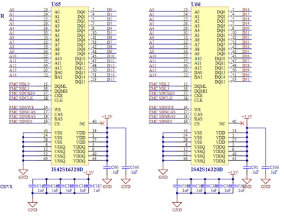
I am using a STM32H743BIT6., I am trying to access two SDRAM part-number(IS42S16320D-7TL)
problem:
both the DRAMS are wring the same data at the same time, so instead of having access to a 32 bit i am getting access to 16bit
help will be apricated
Thank you
Solved! Go to Solution.
- Labels:
-
STM32H7 Series
Accepted Solutions
- Mark as New
- Bookmark
- Subscribe
- Mute
- Subscribe to RSS Feed
- Permalink
- Email to a Friend
- Report Inappropriate Content
2023-11-03 1:26 PM
Perhaps easier to lift leg/pin 20 of both SDRAM and connect to FMC_A15_BA1
So you get the 4x 16MB banks decoding
A13 is not a bank pin
13 rows use (A0..A12)
10 columns use (A0..A9)
Up vote any posts that you find helpful, it shows what's working..
- Mark as New
- Bookmark
- Subscribe
- Mute
- Subscribe to RSS Feed
- Permalink
- Email to a Friend
- Report Inappropriate Content
2023-11-03 10:15 AM
Here is the CubeMX Setting which were used for this test.
@Tesla DeLorean see if you can think of some setting which we might be overlooking here.
- Mark as New
- Bookmark
- Subscribe
- Mute
- Subscribe to RSS Feed
- Permalink
- Email to a Friend
- Report Inappropriate Content
2023-11-03 10:25 AM - edited 2023-11-03 10:40 AM
https://www.mouser.com/datasheet/2/198/42-45R-S_86400D-16320D-32160D-258456.pdf
Suspect the banking is handled incorrectly
FMC_A14/FMC_BA0
FMC_A15/FMC_BA1
These might be usable interchangeably but I think you'll need to change the A13 pin to use A15 as a source instead.
Up vote any posts that you find helpful, it shows what's working..
- Mark as New
- Bookmark
- Subscribe
- Mute
- Subscribe to RSS Feed
- Permalink
- Email to a Friend
- Report Inappropriate Content
2023-11-03 10:44 AM
Thanks, let me try updating that and see if that can make any difference.
- Mark as New
- Bookmark
- Subscribe
- Mute
- Subscribe to RSS Feed
- Permalink
- Email to a Friend
- Report Inappropriate Content
2023-11-03 10:51 AM - edited 2023-11-03 10:51 AM
On the BA0/BA1 side for the SDRAM, I don't suppose which 16MB bank matters to the STM32 provided that it decodes consistently
ie, these will be functionally equivalent
BA0 = A14, BA1 = A15
BA0 = A15, BA1 = A14
In terms of modding the circuit to check, changing one wire seemed the easier option.
Up vote any posts that you find helpful, it shows what's working..
- Mark as New
- Bookmark
- Subscribe
- Mute
- Subscribe to RSS Feed
- Permalink
- Email to a Friend
- Report Inappropriate Content
2023-11-03 11:38 AM
you mean
SDRAM1
A13-----> BA0
A14-----> BA1
SDRAM2
A14-----> BA0
A13-----> BA1
?
- Mark as New
- Bookmark
- Subscribe
- Mute
- Subscribe to RSS Feed
- Permalink
- Email to a Friend
- Report Inappropriate Content
2023-11-03 11:56 AM
No, I mean the bank ordering [0..3] doesn't particularly matter
STM32 A14 = BA0
STM32 A15 = BA1
You've involved STM32 A13, and I don't think that's correct. As you've got A14 already wired to one of the bank pins my suggestion to test was to cut the wire to the other currently carrying A13, and connect that to A15 instead.
I don't see enough of the circuit/schematic to gauge the difficulty to achieving that.
Up vote any posts that you find helpful, it shows what's working..
- Mark as New
- Bookmark
- Subscribe
- Mute
- Subscribe to RSS Feed
- Permalink
- Email to a Friend
- Report Inappropriate Content
2023-11-03 12:07 PM
Hi Tesla DeLorean,
i am attaching a new png file where my A15 is connected to the SRAM. if that won't cause any issues I can modify the change.
- Mark as New
- Bookmark
- Subscribe
- Mute
- Subscribe to RSS Feed
- Permalink
- Email to a Friend
- Report Inappropriate Content
2023-11-03 1:26 PM
Perhaps easier to lift leg/pin 20 of both SDRAM and connect to FMC_A15_BA1
So you get the 4x 16MB banks decoding
A13 is not a bank pin
13 rows use (A0..A12)
10 columns use (A0..A9)
Up vote any posts that you find helpful, it shows what's working..
- Mark as New
- Bookmark
- Subscribe
- Mute
- Subscribe to RSS Feed
- Permalink
- Email to a Friend
- Report Inappropriate Content
2023-11-03 2:06 PM
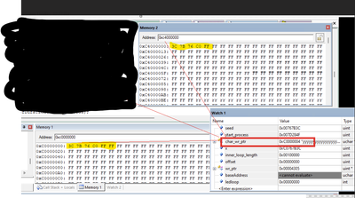
after doing the change to one SDRAM (SDRAM2) we were only able to memset to 0XFFFFFFFF half the memory of SDRAM2 as shown below
do i need to make the change for both the SDRAMS? as you mention A13 is not a bank pin
how to memset the entire memory?
when i am trying to write the SDRAM1 at address 0X0C00000. i can see that some of the data is getting written on address 0X0C10000.
- STM32H7 timer is too slow in STM32 MCUs Products
- Problems with debugging STM32F4 using STM32CubeIDE in STM32CubeIDE (MCUs)
- STM32H743VG Pin PC2_C and PC3_C in STM32 MCUs Products
- Sending UDP on NetXDuo does not work without breakpoints. in STM32 MCUs Products
- extremely slow sdram read write performance in STM32 MCUs Products


