- STMicroelectronics Community
- STM32 MCUs
- STM32 MCUs Products
- Re: DAC noise on SDCARD reads - SOLVED
- Subscribe to RSS Feed
- Mark Topic as New
- Mark Topic as Read
- Float this Topic for Current User
- Bookmark
- Subscribe
- Mute
- Printer Friendly Page
DAC noise on SDCARD reads - SOLVED
- Mark as New
- Bookmark
- Subscribe
- Mute
- Subscribe to RSS Feed
- Permalink
- Email to a Friend
- Report Inappropriate Content
2017-09-03 02:44 PM
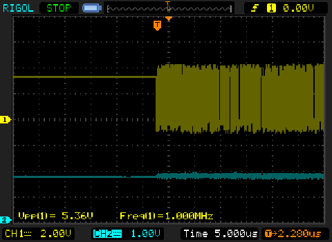
I have a custom board (2 layer) using a STM32F446RETx (3.3v) with STM32CubeMX, V4.22 with firmware V1.16.0. I am reading/processing MP3 files from a sdcard and there is a low-level but perceptible 'thump' in the audio when the card is read. I can change the noise interval by changing the size of the fatfs read buffer. Also see waveform, top trace is SDIO D0 and bottom trace is DAC1

processor speed is 120MHz
SDIO clk 48MHzSDCARD 4-bit with DMA and a lower priority than DACAllowing SDCARD reads but forcing DAC output to a set level (2047) the 'thump' is still heard when the card read takes place. (sounds rather like listening to a heartbeat in a stethoscope).Changing the DAC from 12 bit to 8 bit had no effect.
Enabling or disabling the DAC output buffer has no effect.Changing slew rate on the GPIO pins has no effect.Changing SDIOCLK divisor has no effect.Using 3 different sdcards has no effect.I re-did the board, moving the SDCARD slot away from the CPU and added a 33uF cap across SDCARD pwr supply.SDCARD slot is not under or in close proximity to the MCU and SD traces are not in parallel or close to the DAC traces.The sound quality of the DAC output is fine except for the noise when the card is read.
I thought this would not be a problem since the card and dac are on separate DMA controllers.
Should I give up on using the internal DACs and go with a I2S external DAC?
Thanks for any suggestions.
- Mark as New
- Bookmark
- Subscribe
- Mute
- Subscribe to RSS Feed
- Permalink
- Email to a Friend
- Report Inappropriate Content
2017-09-03 07:01 PM
Managing current flows and power on 2-layer boards is always a nightmare.
Perhaps focus on the bulk and decoupling capacitors on the digital supplies, and what's happening with the VCAP pins.
Perhaps looks at a choke/inductor on the VDDA/VREF+
Other might have a better idea if noise on the die can be reliably kept from the DAC/ADC side of things.
Up vote any posts that you find helpful, it shows what's working..
- Mark as New
- Bookmark
- Subscribe
- Mute
- Subscribe to RSS Feed
- Permalink
- Email to a Friend
- Report Inappropriate Content
2017-09-04 10:13 AM
Thank you for the suggestions Clive1.
I did manage to get a small inductor soldered between V+ and the 1uF cap on VDDA. I also tried changing the 1uF cap to 10uF but in both cases, there was no detectable difference.
Unless someone can say the DAC and SD paths inside the mcu should not interfere with concurrent activity, I think I will try a external DAC next, then failing that, go with the 4-layer board.
- Mark as New
- Bookmark
- Subscribe
- Mute
- Subscribe to RSS Feed
- Permalink
- Email to a Friend
- Report Inappropriate Content
2017-09-04 10:26 AM
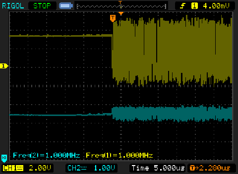
Take a similar scan with the scope than the first one, except that now with VDDA instead of DAC output at channel 2.
JW
- Mark as New
- Bookmark
- Subscribe
- Mute
- Subscribe to RSS Feed
- Permalink
- Email to a Friend
- Report Inappropriate Content
2017-09-04 11:25 AM
Scan with top trace=SDIO D0 and bottom trace=VDDA (at the moment there is a 100nF and a 10uF cap across VDDA).

- Mark as New
- Bookmark
- Subscribe
- Mute
- Subscribe to RSS Feed
- Permalink
- Email to a Friend
- Report Inappropriate Content
2017-09-04 11:40 AM
DAC is only an 'adjustable divider from VDDA'. So make VDDA clean and you're done.
Note that GND is part of the circuit, and that there's nothing like zero resistance track.
JW
- Mark as New
- Bookmark
- Subscribe
- Mute
- Subscribe to RSS Feed
- Permalink
- Email to a Friend
- Report Inappropriate Content
2017-09-04 12:44 PM
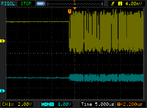
Also trace of VCAP1.

- Mark as New
- Bookmark
- Subscribe
- Mute
- Subscribe to RSS Feed
- Permalink
- Email to a Friend
- Report Inappropriate Content
2017-09-04 08:09 PM
It seems making VDDA clean can't be done with capacitors or inductors.
I think I see a 4-layer board in my future.
Thanks for all the suggestions.
- Mark as New
- Bookmark
- Subscribe
- Mute
- Subscribe to RSS Feed
- Permalink
- Email to a Friend
- Report Inappropriate Content
2017-09-05 01:59 AM
While harder, it's still perfectly possible to achieve the same level of noise on a multilayer board if you don't know what are you doing.
Start with your current board. Cut GND and VCC just next to SDCard. Run two wires to it directly from the regulator. Measure (and be sure you place the ground clip and probe tip to the very same spots as previously). Any change?
JW
- Mark as New
- Bookmark
- Subscribe
- Mute
- Subscribe to RSS Feed
- Permalink
- Email to a Friend
- Report Inappropriate Content
2017-09-05 07:20 PM
I did as you suggested, cut the GND and VCC connections to the SDCARD and ran wires to the regulator. Unfortunately, the noise is same or more so with the board in this state. The SDCARD still has a full ground plane under it so it may still be inducing something there. I will say it seems odd the scope trace from before shows the noise as being high in frequency but what I hear is actually fairly low but I suppose some kind of aliasing could explain that.
I may try one more 2-layer board but remove the ground plane from under the card and run separate traces back as I did with the wires. At least I now feel confident this is not a problem with concurrent DMA activity.
Thank you.
- STM32WL33 Boot Loader and startup in STM32 MCUs Wireless
- SDMMC FATFS and TouchGfx Memory Issues in STM32 MCUs Embedded software
- SD-card Works in 1-bit mode but it does not work in 4- bit mode. in STM32 MCUs Embedded software
- Severe error in Azure RTOS FileX, corrupts memory, solution in STM32 MCUs Embedded software
- [SOLVED] - Simple temperature sensor I2C reading gives bizarre incorrect reading in STM32 MCUs Products