- STMicroelectronics Community
- STM32 MCUs
- STM32 MCUs Products
- Clock cycle shift on GPIO output STM32F103
- Subscribe to RSS Feed
- Mark Topic as New
- Mark Topic as Read
- Float this Topic for Current User
- Bookmark
- Subscribe
- Mute
- Printer Friendly Page
Clock cycle shift on GPIO output STM32F103
- Mark as New
- Bookmark
- Subscribe
- Mute
- Subscribe to RSS Feed
- Permalink
- Email to a Friend
- Report Inappropriate Content
2024-05-11 9:49 PM
Dear Community,
I am porting an old application made on AVR to STM32, and I am facing a strange timing issue.
In a nutshell, the application is reading sector (512 Bytes) from a SDCARD and output the content of the buffer to GPIO with 4us cycle (meaning 3us low, 1 us data signal).
The SDCard read is working fine, and I have written a small assembly code to output GPIO signal with precise MCU cycle counting.
Using DWT on the debugger, it give a very stable and precise counting (288 cycles for a total of 4us).
When using a Logic analyser with 24 MHz freq, I can see shift of signal by 1 or 2 cpu cycles and so delay.
I have tried to use ODR directly and BSRR but with no luck.
Attached :
- Screenshot of the logic analyzer

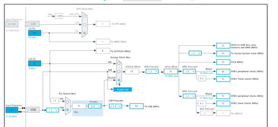
Clock configuration
Port configuration:
I do not know where to look at to be honnest
- Labels:
-
STM32F1 Series
- Mark as New
- Bookmark
- Subscribe
- Mute
- Subscribe to RSS Feed
- Permalink
- Email to a Friend
- Report Inappropriate Content
2024-05-28 12:28 AM
Ok I found it :
It needs to have
void HAL_SPI_TxCpltCallback(SPI_HandleTypeDef *hspi)
{
  printf("debug full\n");
}


void HAL_SPI_TxHalfCpltCallback(SPI_HandleTypeDef *hspi){
   printf("debug half\n");
}
along with
HAL_SPI_Transmit_DMA(&hspi1,DMA_BIT_BUFFER,1608); // 402*8*4By the way the DMA_SPI_TX seems to be the best approach to save RAM and very precise & accurate
Vincent
- « Previous
- Next »
- PWM input output drift in STM32 MCUs Products
- Motor Control Workbench Position Control: Proper way to reset theta. in STM32 MCUs Motor control
- SSI Slave on a STM32H743 via SPI in STM32 MCUs Products
- STM32F103C8 PWM and clock slow down and MCU restarts in noisy environment. in Others: STM32 MCUs related
- MIPI-DSI: Image shift occasionnally in STM32 MCUs TouchGFX and GUI
