ADC acquisition time
- Mark as New
- Bookmark
- Subscribe
- Mute
- Subscribe to RSS Feed
- Permalink
- Email to a Friend
- Report Inappropriate Content
2019-12-16 10:19 PM
Hello everyone,
Where can i get the ADC acquisition time for stm32h753_tfbga100 IC??
- Labels:
-
ADC
-
STM32H7 Series
- Mark as New
- Bookmark
- Subscribe
- Mute
- Subscribe to RSS Feed
- Permalink
- Email to a Friend
- Report Inappropriate Content
2019-12-16 11:13 PM
Datasheet / reference manual ?
- Mark as New
- Bookmark
- Subscribe
- Mute
- Subscribe to RSS Feed
- Permalink
- Email to a Friend
- Report Inappropriate Content
2019-12-17 3:44 AM
Hello Ozone,
I didnt find anything about acquisition time in the datasheet.
Is there any methods to calculate the ADC acquisition time??
- Mark as New
- Bookmark
- Subscribe
- Mute
- Subscribe to RSS Feed
- Permalink
- Email to a Friend
- Report Inappropriate Content
2019-12-17 3:56 AM
There are no fixed acquisition times with STM32 ADCs. Pretty sure the H7 is not different.
It is called sampling time here, and can be configured as a number of ADC clock cycles.
So, define your ADC peripheral clock, and set the sampling time for each channel according to your needs.
Details are usually in the reference manual.
- Mark as New
- Bookmark
- Subscribe
- Mute
- Subscribe to RSS Feed
- Permalink
- Email to a Friend
- Report Inappropriate Content
2019-12-17 6:10 AM
As Ozone said above, there's no fixed time, it depends on configuration.
Total conversion time depends on
- ADC clock selection (ADCx_CCR.CKMODE and respective registers in RCC)
- ADC clock prescaler (ADCx_CCR.PRESC)
- sampling time selection (ADC_SMPRx.SMPx)
- resolution selected (ADC_CFGR.RES)
You can also configure ADCs to convert in interleaved mode on the same source, which may effectively act as shorter total conversion time.
Read the ADC chapter in AN. The ADC in the 'H7 is very complex.
JW
- Mark as New
- Bookmark
- Subscribe
- Mute
- Subscribe to RSS Feed
- Permalink
- Email to a Friend
- Report Inappropriate Content
2019-12-17 10:00 PM
Hi Ozone, waclawek.jan
Thanks for the Info, but I am finding it bit complicated to get soluiton from the AN. So let me explain what i am searching for.
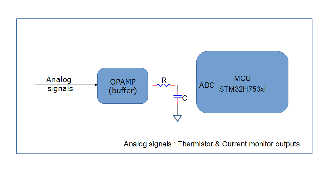
I am planning to read the sensor data through ADC lines. An OPAMP buffer and an RC network is connected in between sensor and MCU.
Since the addition of opamp may induce capacitive loading, I am confused with the RC value so that it wont effect the ADC operation of MCU.
The circuit is shared below.
Kindly, let me know your inputs.
- Mark as New
- Bookmark
- Subscribe
- Mute
- Subscribe to RSS Feed
- Permalink
- Email to a Friend
- Report Inappropriate Content
2019-12-18 12:39 AM
The ADC input of mcu can be modeled as a capacitor (capacitance to be found in datasheet (DS), around 6-10pF), which (during the previous conversion) is internally charged to an arbitrary voltage between 0 and VDDA (typically VDDA/2) and then switched to the input pin for the duration of the sampling time (which as I've explained above is up to you how do you set up).
Your task is to design the input circuit so that this capacitor is charged to your desired input voltage within the time given by the sampling time, to within an error you desire.
JW
- Mark as New
- Bookmark
- Subscribe
- Mute
- Subscribe to RSS Feed
- Permalink
- Email to a Friend
- Report Inappropriate Content
2019-12-18 3:13 AM
> Since the addition of opamp may induce capacitive loading, I am confused with the RC value so that it wont effect the ADC operation of MCU.
The ADC operation will be affected if the input (sensor, opamp) does not deliver enough current to charge/uncharge the S&H capacitor quickly enough, and the conversion result will depend on the previous channel (residual charge), which looks like channel crosstalk.
As jan mentioned, this is a simple RC element calculation. The internal R and C values are defined in the datasheet, ADC section. Add the output impedance of your buffer opamp to that.
With thermistors, you would need at most a few samples per second. I would go for a long sampling time.