- STMicroelectronics Community
- STM32 MCUs
- STM32 MCUs Products
- Re: A question about Vdd, VddA, Vref and clock fre...
- Subscribe to RSS Feed
- Mark Topic as New
- Mark Topic as Read
- Float this Topic for Current User
- Bookmark
- Subscribe
- Mute
- Printer Friendly Page
A question about Vdd, VddA, Vref and clock frequencies
- Mark as New
- Bookmark
- Subscribe
- Mute
- Subscribe to RSS Feed
- Permalink
- Email to a Friend
- Report Inappropriate Content
2019-07-12 01:51 AM
Hello,
we want to build a system with STM32H7, hopefully one of the new up to 480 MHz devices. And we really need a high clock of 400 MHz and above. On the other hand we need low power and we use ADC and DAC, both requiring a 3.3V Vref.
Now my question is if we can turn down Vdd to 1.8V to minimize the power loss in LDO voltage regulator, while keeping VddA and Vref at 3.3V.
I searched the data sheets but couldn't find any relations between Vdd and VddA. (which would be a yes to my question but still leaves me a bit insecure, maybe I missed something)
Thanks for any help
Martin
Solved! Go to Solution.
- Labels:
-
STM32H7 Series
Accepted Solutions
- Mark as New
- Bookmark
- Subscribe
- Mute
- Subscribe to RSS Feed
- Permalink
- Email to a Friend
- Report Inappropriate Content
2019-07-12 03:52 AM
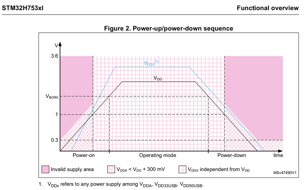
Section 3.5.2 and Figure 2 in the stm32h753 data sheet (rev 7) seems to show some restrictions on VddA vs Vdd during the power-up / power-down sequence.
Essentially they say that all the time Vdd < 1.0 V, VddA (and VddUSB) need to be below Vdd + 0.3 V.
During power-up and power-down phases, the following power sequence requirements must be respected (see Figure 2):
- When VDD is below 1 V, other power supplies (VDDA, VDD33USB, VDD50USB) must remain below VDD + 300 mV.
When VDD is above 1 V, all power supplies are independent.
- During the power-down phase, VDD can temporarily become lower than other supplies only if the energy provided to the microcontroller remains below 1 mJ. This allows external decoupling capacitors to be discharged with different time constants during the power-down transient phase.
- Mark as New
- Bookmark
- Subscribe
- Mute
- Subscribe to RSS Feed
- Permalink
- Email to a Friend
- Report Inappropriate Content
2019-07-12 05:54 AM
Danish,
thank you for this hint, I was missing this part.
Thanks a lot
Martin
- STM32WBA52 ADC Maximum Clock Frequency & Max Sample Rate at 12-Bit Resolution in STM32 MCUs Wireless
- Block Erase Function Issue with MT25QL01GBBB NOR Flash on STM32 MCU in STM32 MCUs Products
- Need for series resistors for OCTOSPI on NucleoU5A5 in STM32 MCUs Products
- Questions on how RTC clock usage STM32F103 in STM32 MCUs Products
- stm32f4 interrupts and i2c in STM32 MCUs Products
