- STMicroelectronics Community
- STM32 MCUs
- STM32 MCUs Embedded software
- Re: STM32H7 MIPI DSI maximum clock speed?
- Subscribe to RSS Feed
- Mark Topic as New
- Mark Topic as Read
- Float this Topic for Current User
- Bookmark
- Subscribe
- Mute
- Printer Friendly Page
STM32H7 MIPI DSI maximum clock speed?
- Mark as New
- Bookmark
- Subscribe
- Mute
- Subscribe to RSS Feed
- Permalink
- Email to a Friend
- Report Inappropriate Content
2020-02-29 09:17 AM
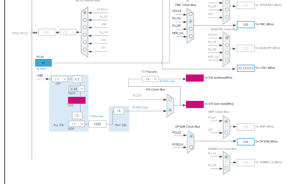
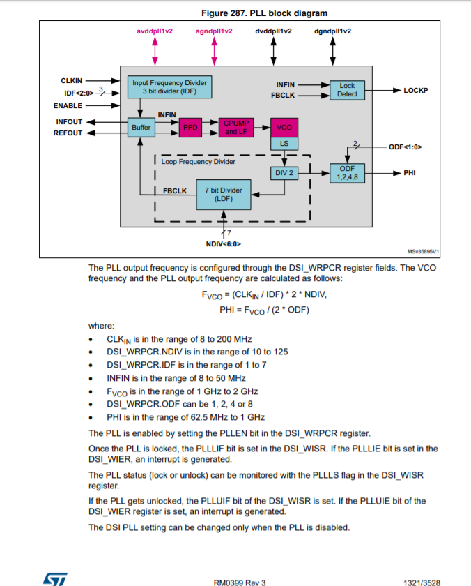
There is inconsistency in the reference manual and the STM32CubeMX clock configuration tool as to what the maximum clock for the PLL DSI. Reference manual suggests it is 1000 MHz however, when set to that in STM32CubeMX, an error is generated at the PHY DSI lane byte frequency with a maximum of 62MHz instead of an expected 125MHz
- Labels:
-
Audio
-
Documentation
-
DSI
-
STM32CubeMX
-
STM32H7 Series
- Mark as New
- Bookmark
- Subscribe
- Mute
- Subscribe to RSS Feed
- Permalink
- Email to a Friend
- Report Inappropriate Content
2020-02-29 10:48 AM
Not 1 GHz, but 1 Gbps via both edges on both lanes
Up vote any posts that you find helpful, it shows what's working..
- Mark as New
- Bookmark
- Subscribe
- Mute
- Subscribe to RSS Feed
- Permalink
- Email to a Friend
- Report Inappropriate Content
2020-02-29 10:59 AM - edited 2024-09-23 01:43 PM
62 MHz is more of the word delivery clock
62.5 MHz 32-bpp
83.3 MHz 24-bpp
DSI HOST, 500 MHz clock, signal on both edges, 1x lane 1 Gbps, 2x lane 2 Gbps
2000/24 -> 83.333
Up vote any posts that you find helpful, it shows what's working..
- Mark as New
- Bookmark
- Subscribe
- Mute
- Subscribe to RSS Feed
- Permalink
- Email to a Friend
- Report Inappropriate Content
2020-02-29 11:28 AM
Yes its DDR on the output clock at but according to the RM the PLL puts out 1GHz. When using those setting CubeMX gives an error so I'm not sure if there is a hardware limitation or just software bug in CubeMX. Don't have hardware yet so can't test at the moment.
- Mark as New
- Bookmark
- Subscribe
- Mute
- Subscribe to RSS Feed
- Permalink
- Email to a Friend
- Report Inappropriate Content
2024-09-23 01:22 PM
For STM32H7 it is 1Gbps per lane - 2Gbps total.
- Mark as New
- Bookmark
- Subscribe
- Mute
- Subscribe to RSS Feed
- Permalink
- Email to a Friend
- Report Inappropriate Content
2024-09-27 08:53 AM
- Mark as New
- Bookmark
- Subscribe
- Mute
- Subscribe to RSS Feed
- Permalink
- Email to a Friend
- Report Inappropriate Content
2024-11-12 01:00 PM
Ahh, yeah, I mean dual core STM32H7 MCUs:
From STM32H747 datasheet:
From AN4860:
- Mark as New
- Bookmark
- Subscribe
- Mute
- Subscribe to RSS Feed
- Permalink
- Email to a Friend
- Report Inappropriate Content
2024-11-12 02:39 PM
Because it's not funnelling BITS into the pipe it's either 16 or 24-bit words for the PIXEL. The 62.5 MHz is the PIXEL clock, the LTDC spits out the data as it paints the rasters, and the DSI needs to move it out at least that quickly.
The DSI PHY clocks at the high rate to push BITS out the LANES, 1 GHz in there is basically 500 MHz on the DSI bus itself.
62.5 MHz / 50 Hz refresh = 1.25 Mpixel
Up vote any posts that you find helpful, it shows what's working..
- Mark as New
- Bookmark
- Subscribe
- Mute
- Subscribe to RSS Feed
- Permalink
- Email to a Friend
- Report Inappropriate Content
2024-11-20 01:17 PM
Four years on and the confusion is still here. It's unclear whether this is a bug in CubeMX or a hardware limitation.
- STM32H7 HAL: possible bug in HAL_RCC_GetPCLK1Freq()? Incorrect UART baudrate generation in STM32 MCUs Embedded software
- STM32WBA52 ADC Maximum Clock Frequency & Max Sample Rate at 12-Bit Resolution in STM32 MCUs Wireless
- STM32H7 SDRAM Speed Code and CAS Latency in STM32 MCUs Products
- Is speed control impossible in motor position control? in STM32 MCUs Motor control
- HSO recommended hardware setup in STM32 MCUs Motor control


