- STMicroelectronics Community
- STM32 MCUs
- STM32 MCUs Boards and hardware tools
- Re: STM32f103vdt6 design
- Subscribe to RSS Feed
- Mark Topic as New
- Mark Topic as Read
- Float this Topic for Current User
- Bookmark
- Subscribe
- Mute
- Printer Friendly Page
STM32f103vdt6 design
- Mark as New
- Bookmark
- Subscribe
- Mute
- Subscribe to RSS Feed
- Permalink
- Email to a Friend
- Report Inappropriate Content
2019-10-16 08:16 AM
Hello!
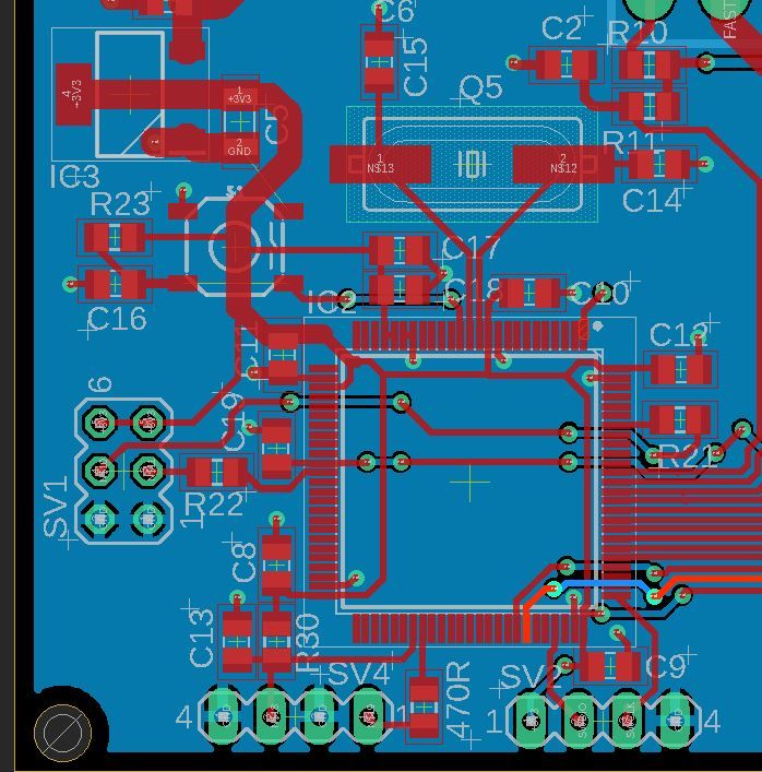
I have designed a custom board, i have attached the schematic of it. My problem is that I have an ST-link v2 and i cant connect to it, i get target not found. Is my schematic correct or I have missed something? I have power and ground on all necessary pins on my board. I connected VDD, GND, SWDIO and SWCLK to my board from the ST-link, I used pins 1, 7, 9, 20. I tried to swap the pins of the data and clock signals, and all the settings in the ST-Link utility. My programmers firmware is up to date.
Best regards,
Attila
Solved! Go to Solution.
- Labels:
-
STM32F1 Series
Accepted Solutions
- Mark as New
- Bookmark
- Subscribe
- Mute
- Subscribe to RSS Feed
- Permalink
- Email to a Friend
- Report Inappropriate Content
2019-10-16 03:27 PM
That chip is upside down.
With the text right side up, pin 1 is at the bottom left on the chip.
Agreed, it's confusing with two marks.
- Mark as New
- Bookmark
- Subscribe
- Mute
- Subscribe to RSS Feed
- Permalink
- Email to a Friend
- Report Inappropriate Content
2019-10-16 08:28 AM
Check the voltages
Check part orientation
Check level on NRST pin
With BOOT0 pulled high try talking to the ROM based System Loader, via USART1 PA9/PA10, at 9600 8E1 send an 0x7F data byte, and check for response. Use something like RealTerm which can send hex bytes.
Up vote any posts that you find helpful, it shows what's working..
- Mark as New
- Bookmark
- Subscribe
- Mute
- Subscribe to RSS Feed
- Permalink
- Email to a Friend
- Report Inappropriate Content
2019-10-16 08:53 AM
VBAT should be connected to VCC.
Is pin 73 really NC on the package? Seems odd.
- Mark as New
- Bookmark
- Subscribe
- Mute
- Subscribe to RSS Feed
- Permalink
- Email to a Friend
- Report Inappropriate Content
2019-10-16 08:57 AM
I have checked the voltages, all ok. The part oriantation indentation is in the up right corner. For some reason the NRST is 0.26V, but if I put a wire I can bring it up to 3.2V. But still no luck. I tried with an arduino the BOOT0 method with 0x7F data byte. I checked the answer on the oscilloscope and there was some response data.
- Mark as New
- Bookmark
- Subscribe
- Mute
- Subscribe to RSS Feed
- Permalink
- Email to a Friend
- Report Inappropriate Content
2019-10-16 08:59 AM
I tried that too, with no luck. If Im correct it is NC, I attach the datasheet.
- Mark as New
- Bookmark
- Subscribe
- Mute
- Subscribe to RSS Feed
- Permalink
- Email to a Friend
- Report Inappropriate Content
2019-10-16 09:00 AM
If NRST wants to be 0.26V, voltages are not okay. Indicates a problem in your power supply scheme somewhere.
- Mark as New
- Bookmark
- Subscribe
- Mute
- Subscribe to RSS Feed
- Permalink
- Email to a Friend
- Report Inappropriate Content
2019-10-16 09:19 AM
This is akward for me too, and the second odd thing is that PA2 is shorted to VDD in the interior of the IC. But I measured the voltages on all the pins and are ok.
- Mark as New
- Bookmark
- Subscribe
- Mute
- Subscribe to RSS Feed
- Permalink
- Email to a Friend
- Report Inappropriate Content
2019-10-16 12:39 PM
Did you measure *directly* on the pins? I am aiming at bad solder joints.
Did you measure also VDDA/VSSA?
Is the text on the chip bottom-up?
JW
- Mark as New
- Bookmark
- Subscribe
- Mute
- Subscribe to RSS Feed
- Permalink
- Email to a Friend
- Report Inappropriate Content
2019-10-16 01:28 PM
Definately sounds like you've got the device rotated.
NRST will be low absent a VDDA supply on the correct pin.
Show clear, in focus, high resolution photo of the chip on the board.
Don't confuse the mold ejector marks for pin 1 designation
Up vote any posts that you find helpful, it shows what's working..
- Mark as New
- Bookmark
- Subscribe
- Mute
- Subscribe to RSS Feed
- Permalink
- Email to a Friend
- Report Inappropriate Content
2019-10-16 03:20 PM
Yeah. I have thinked about this, and I measured all the voltages on the top of the pins, near the package with really thin probes. I measured all of the vdd/vss pins. No, the text is up-buttom.
- STM32CubeProgrammer not working with STM32F072 for USB DFU in STM32CubeProgrammer (MCUs)
- Cannot make STLINK v2 connection with STM32WL33 in STM32CubeProgrammer (MCUs)
- STM32H573 VFQFPN68 exposed pad details in STM32 MCUs Boards and hardware tools
- Using integrated DB function of STM32U5 with TCPP01-M12 in STM32 MCUs Products
- Using Hex file or Bin file for FOTA? in STM32 MCUs Products

