- STMicroelectronics Community
- MEMS and sensors
- MEMS (sensors)
- Re: LIS2DH12TR PLEASE CONFIRM WHY THERE IS NO BODY...
- Subscribe to RSS Feed
- Mark Topic as New
- Mark Topic as Read
- Float this Topic for Current User
- Bookmark
- Subscribe
- Mute
- Printer Friendly Page
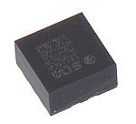
LIS2DH12TR PLEASE CONFIRM WHY THERE IS NO BODY MARK OVER THIS MOTION SENSOR IC.
- Mark as New
- Bookmark
- Subscribe
- Mute
- Subscribe to RSS Feed
- Permalink
- Email to a Friend
- Report Inappropriate Content
2021-02-23 11:30 PM
Solved! Go to Solution.
Accepted Solutions
- Mark as New
- Bookmark
- Subscribe
- Mute
- Subscribe to RSS Feed
- Permalink
- Email to a Friend
- Report Inappropriate Content
2021-02-24 12:38 AM
Hi @USING.1 ,
there should be a indeed a marking on the top surface of the device package, like the one here below:

-Eleon
- Mark as New
- Bookmark
- Subscribe
- Mute
- Subscribe to RSS Feed
- Permalink
- Email to a Friend
- Report Inappropriate Content
2021-02-24 12:38 AM
Hi @USING.1 ,
there should be a indeed a marking on the top surface of the device package, like the one here below:

-Eleon
- Mark as New
- Bookmark
- Subscribe
- Mute
- Subscribe to RSS Feed
- Permalink
- Email to a Friend
- Report Inappropriate Content
2021-02-24 01:10 AM
Thanks for reply. But this is not mentioned anywhere in datasheet. Please clarify ?
- Mark as New
- Bookmark
- Subscribe
- Mute
- Subscribe to RSS Feed
- Permalink
- Email to a Friend
- Report Inappropriate Content
2021-02-24 02:37 AM
Hi @USING.1 ,
no, it is not specified in the datasheet...
This because the datasheet is generic, while the 2D matrix is related to the specific assy lot for the case tracking (it contains the product code, the week/year (usually in the format Y/WW) of assy etc...).
-Eleon
- Mark as New
- Bookmark
- Subscribe
- Mute
- Subscribe to RSS Feed
- Permalink
- Email to a Friend
- Report Inappropriate Content
2021-02-24 02:42 AM
Thanks Mr Borlini for your prompt replies.
- Mark as New
- Bookmark
- Subscribe
- Mute
- Subscribe to RSS Feed
- Permalink
- Email to a Friend
- Report Inappropriate Content
2021-02-24 02:47 AM
You're welcome @USING.1 , hope this could be of some help for you.
-Eleon
- LSM6DSV16X Sensor Fusion (SFLP): Does It Use Filtered or Raw Data? in MEMS (sensors)
- LPS22HBTR pressure range query in MEMS (sensors)
- LIS2MDL BDU only works for 3 axis independent readouts in MEMS (sensors)
- STSW-IMG506 - libcamera IPA package for ST BrightSense image sensors failing on Raspberry Pi in Imaging (sensors)
- LSM6DSV16X Gyroscope bias in MEMS (sensors)