- STMicroelectronics Community
- STM32 MCUs
- STM32 MCUs Boards and hardware tools
- Correct way to remove ST-Link from Nucleo-F401RE, ...
- Subscribe to RSS Feed
- Mark Topic as New
- Mark Topic as Read
- Float this Topic for Current User
- Bookmark
- Subscribe
- Mute
- Printer Friendly Page
Correct way to remove ST-Link from Nucleo-F401RE, also did I destroy my board...
- Mark as New
- Bookmark
- Subscribe
- Mute
- Subscribe to RSS Feed
- Permalink
- Email to a Friend
- Report Inappropriate Content
2015-11-21 06:23 PM
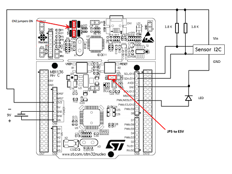
I prepared the circuit in the attached image and planned to remove the ST-Link part of the board to finish my project. Before doing this (because I messed it up last time) I checked that I could externally power the board with a 9-volt battery. Before applying the voltage I disconnected from usb power and moved the JP6 jumper from U5V to E5V. I plugged in the battery and everything worked fine.....but then I decided to change some code.
I removed the 9-volt, set the jumper back. Then I connected ST-Link to my PC again by usb and now nothing works. I get a FAIL message in the Nucleo ''The interface firmware FAILED to reset/halt the target MCU
'' and the ST-Link utility tells me''
Cannot read memory!
Disable Read Out Protection and retry.
''Is one of the boards now bad? Is it in some state that is reversible? What is the best way remove the st-link part of the board? #swd #nucleo #st-link
- Mark as New
- Bookmark
- Subscribe
- Mute
- Subscribe to RSS Feed
- Permalink
- Email to a Friend
- Report Inappropriate Content
2015-11-22 04:39 PM
https://developer.mbed.org/forum/team-79-ST-community/topic/16810/?page=1#comment-39697
) and I see data without an error. This post also suggests that the option bytes need to be set to 0..but STlink utility won't do it because of the read read out protection... how can I reset this?- Mark as New
- Bookmark
- Subscribe
- Mute
- Subscribe to RSS Feed
- Permalink
- Email to a Friend
- Report Inappropriate Content
2015-11-22 08:33 PM
You removed JP1 ??
I'm not sure there is a remedy for toasted silicon. My sense is that most people with this type of fault have damaged their boards in some fashion. ie complain about this error, and when you drill down they did something before that, which often involved injecting high voltages in the wrong places.I'd suggest you check the voltages coming off the regulators.Up vote any posts that you find helpful, it shows what's working..
- Mark as New
- Bookmark
- Subscribe
- Mute
- Subscribe to RSS Feed
- Permalink
- Email to a Friend
- Report Inappropriate Content
2015-11-22 09:57 PM
Out of the box JP1 was open. I hope to learn from this but I don't know where I went wrong. I have another board on order and want to avoid this in the future.
I injected 9v to Vin and GND, the circuit worked until I tried to go back to USB at JP5.I couldn't derive from documentation how to separate the stlink, nor how to use it to program after it is removed.- Mark as New
- Bookmark
- Subscribe
- Mute
- Subscribe to RSS Feed
- Permalink
- Email to a Friend
- Report Inappropriate Content
2015-11-23 08:28 AM
I couldn't derive from documentation how to separate the stlink, nor how to use it to program after it is removed.
I simply cut mine off using a small band saw. Then I filed the cut edges on both boards a bit to make sure the exposed leads weren't shorted to each other by copper fragments. When you are done, the ST-Link part is used as a PC USB to SWD programmer using your fabricated jumpers from CN2 (correction : SWD connector) to the correct pins on whatever board you are programming and separately powering. The User Manual defines jumper settings for SWD programming. Cheers, Hal- Mark as New
- Bookmark
- Subscribe
- Mute
- Subscribe to RSS Feed
- Permalink
- Email to a Friend
- Report Inappropriate Content
2015-11-23 01:20 PM
- Mark as New
- Bookmark
- Subscribe
- Mute
- Subscribe to RSS Feed
- Permalink
- Email to a Friend
- Report Inappropriate Content
2015-11-23 01:54 PM
The manual does suggest that 9V should be viable in the configuration you suggest. I haven't had cause to break my Nucleo's apart or externally power them. Not really sure what would cause the part to indicate it is locked.
Up vote any posts that you find helpful, it shows what's working..
- L6470 Stepper Driver - Large cap on VS to ground destroyed?? in STM32 MCUs Motor control
- How to program STM32C011J6M6 in SO8 in STM32 MCUs products
- I2C How to switch between receive and transmit Interrupt the rigth way? | I2C VS SMBUS | STM32F446RE Raspberry in STM32 MCUs products
- calling screen interactions via using function pointers in STM32 MCUs TouchGFX and GUI
- STM32H743 TCP-IP fault (FreeRTOS LwIP) in STM32 MCUs Embedded software