- STMicroelectronics Community
- STM32 MCUs
- STM32 MCUs Boards and hardware tools
- stm32f7 custom pcb
- Subscribe to RSS Feed
- Mark Topic as New
- Mark Topic as Read
- Float this Topic for Current User
- Bookmark
- Subscribe
- Mute
- Printer Friendly Page
stm32f7 custom pcb
- Mark as New
- Bookmark
- Subscribe
- Mute
- Subscribe to RSS Feed
- Permalink
- Email to a Friend
- Report Inappropriate Content
2018-02-27 11:37 AM
Hey everyone,
This is going to be a lengthy post but any help will really be appreciated!!
I'd like to integrate the MCU that I've been using into my final system(i.e no dev board)
I've designed PCB's in the past, but this feels a little more up there, so I just want a few checks
I've read the documentation although this is what I've gathered:
Documents used:
This is an overview of me designing the necessary hardware to get a device up and running. I have a few questions that I laid down in each section. I've split it into the same sections that the ''
'' application note covers.Power supplies:
The device needs a supply of 1.8V to 3.6 V.
http://www.analog.com/media/en/technical-documentation/data-sheets/ADM7pdf
.I'll connect this to all peripheral supplies of the device(sdmmc and usb, etc.), therefore I can ignore the
I've also followed the following overview of the power supplies for the stm32f722ze:
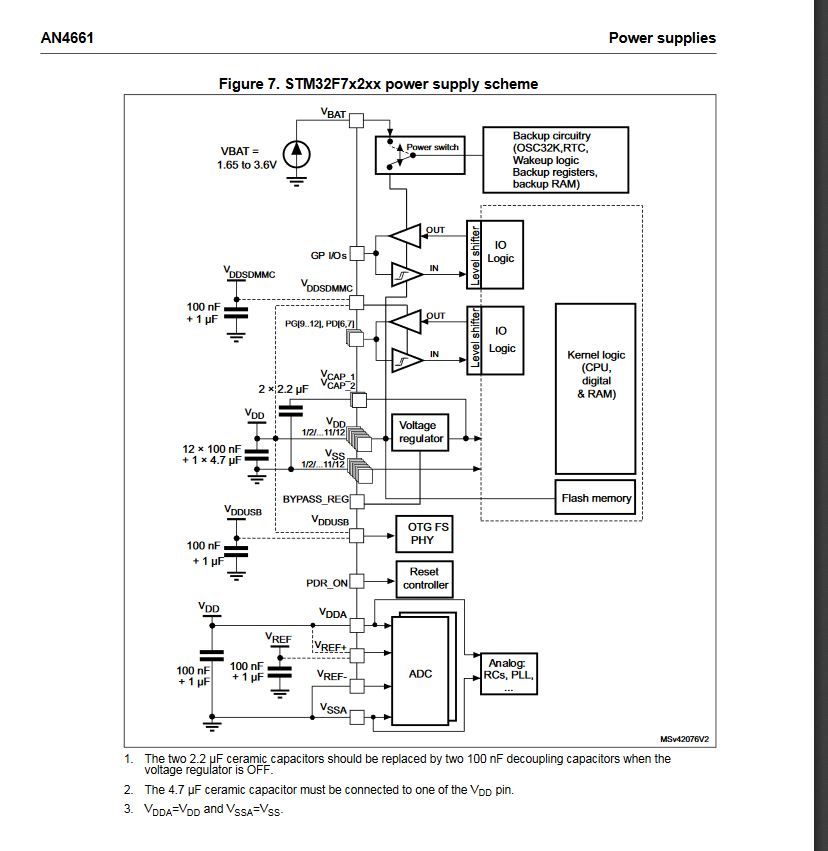
And I've added all the specified parallel capacitors and followed the footnotes shown.
Voltage regulator:
Looking at my technical manual it refers to the pin for activation asPower supply supervisor:
I've set the power supply supervisor to be on and plan on using an external battery to run the RTC during low power modes.
Clocks
On startup the device uses the internal 16 MHz clock, after which a external clock (4 - 26 MHZ) can be selected. This will be scaled to 216 MHz using the PLL's within the device.
https://www.digikey.com/product-detail/en/ecs-inc/ECS-2520S33-250-FN-TR/XC2198CT-ND/6578505
for the main clockFurther a LSE clock can also be externally used.This will allow for the RTC to have a very accurate clock/calendar and for other timing functions.
https://www.mouser.co.za/ProductDetail/?qs=sFmtmVcT%2ffvMvdzcXdd8BQ==
Boot mode
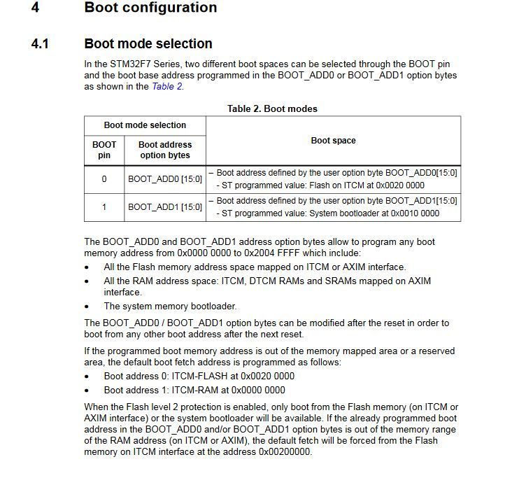
For the bootmode, there are a few different sequences shown in the manuals and application note an26
patterns that can be applied depending on the chip. . I'm not sure how to apply this to the board though.I've read the following section from the ''Getting started with STM32F7 Series MCU hardware development'' application note. It seems that setting pin boot0 to 0V loads from flash and setting pin boot0 loads from flash? I'm not too sure about this though.
Debug management
To debug the board I plan on implementing the ST link that the nucloes come with.
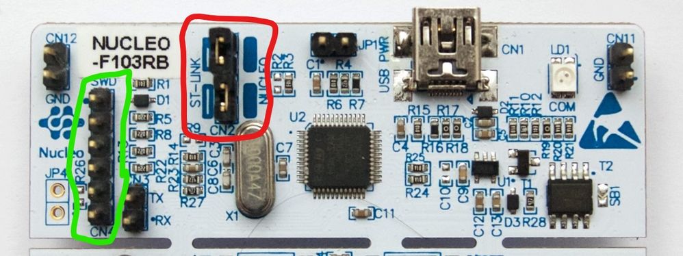
It seems that I only need to decouple the jumpers(shown in red) and then use the swd pins shown in green to debug the board. I'll couple the pins shown in green to my custom board.
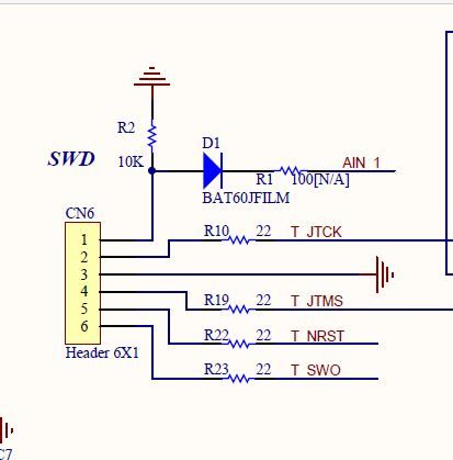
Looking at the nucleo-f722ze schematic for the header pins (shown above), I'm assuming I only need the following pins:
pin 2 : T_JTCK (SWCLK)
pin3 : connect to ground
pin 4 : T_JTMS (SWDIO)
Thanks in advance for any help, I really appreciate it
arm-cortex-m7 pcb-assembly pcb-design stm32f7Solved! Go to Solution.
- Labels:
-
STM32F7 Series
Accepted Solutions
- Mark as New
- Bookmark
- Subscribe
- Mute
- Subscribe to RSS Feed
- Permalink
- Email to a Friend
- Report Inappropriate Content
2018-02-27 03:22 PM
It is a long learning curve. I use Kicad and Visual Studio
The RTC, to make that have any chance of being accurate, you must bake the board after manufacture and coat the capacitors to stop any humidity effects. It is unlikely that you will be able to use the RTC beyond a few days. before the time is incorrect for the next 2 years. I suggest a DS3232 for super accurate RTC.
Which package will you look at ? 144 pin.. good
I use the LQFPs to be sure I can rework the prototypes easily.
Also it offers the cost benefit of a 2 layer board.
otherwise, your steps above look good.
I used a reset chip to avoid all the startup stabilization
- Mark as New
- Bookmark
- Subscribe
- Mute
- Subscribe to RSS Feed
- Permalink
- Email to a Friend
- Report Inappropriate Content
2018-02-27 01:47 PM
In addition to the jumpers marked in RED, one should also watch for SWO, NRESET which have common connectivity with the target. Check solder bridges to achieve more complete disconnection.
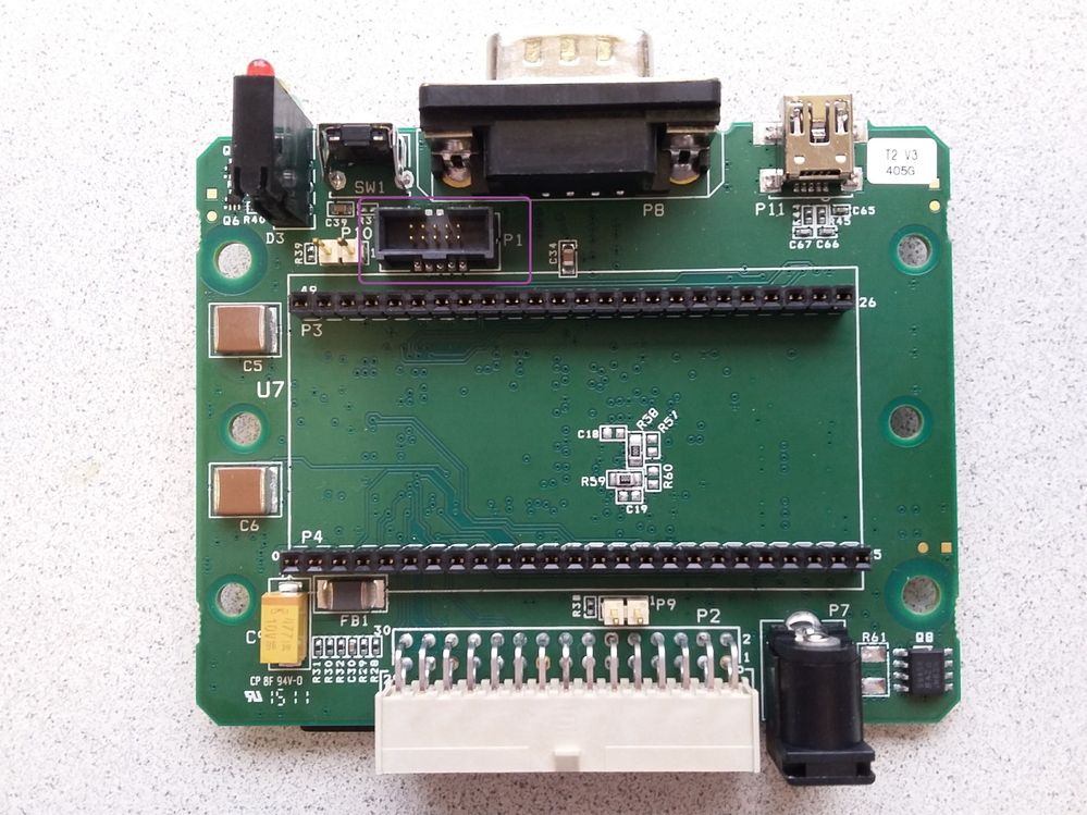
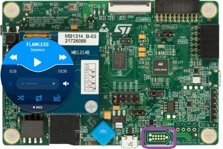
I would generally recommend using a standard 10-pin SWD connector, or older style 20-pin JTAG (SWDIO, SWCLK, SWO, NRESET subset). The local FAE likes the Tag-Connect system and some of the newer DISCO boards have such foot prints. I like edge castellations over test points.
Up vote any posts that you find helpful, it shows what's working..
- Mark as New
- Bookmark
- Subscribe
- Mute
- Subscribe to RSS Feed
- Permalink
- Email to a Friend
- Report Inappropriate Content
2018-02-27 03:22 PM
It is a long learning curve. I use Kicad and Visual Studio
The RTC, to make that have any chance of being accurate, you must bake the board after manufacture and coat the capacitors to stop any humidity effects. It is unlikely that you will be able to use the RTC beyond a few days. before the time is incorrect for the next 2 years. I suggest a DS3232 for super accurate RTC.
Which package will you look at ? 144 pin.. good
I use the LQFPs to be sure I can rework the prototypes easily.
Also it offers the cost benefit of a 2 layer board.
otherwise, your steps above look good.
I used a reset chip to avoid all the startup stabilization
- Mark as New
- Bookmark
- Subscribe
- Mute
- Subscribe to RSS Feed
- Permalink
- Email to a Friend
- Report Inappropriate Content
2018-02-28 09:35 AM
Hi
Marsh.Nick
,Thank you for the help.
I have a few questions on the accuracy of the RTC just to expand my knowledge(if you dont mind). Why would it drift that substantially, I thought choosing a low value for frequency stability would be all that needs to be done? Also why would baking it instead of soldering help with this?
I'll look into the RTC provided, Ideally I'd like to have it have an alarm to trigger events during periods(As I want the device to be triggered every ten minutes between 8 am to 5 pm and then switch to a low power mode), it does seem that a few devices provided integrated alarms.
Just another question. I'm a little lost on the boot configuration. If I'd like to boot from flash, I'm assuming all I need to do is set the boot0 to 0V?
T J wrote:
I used a reset chip to avoid all the startup stabilizationFinally, what exactly would a reset chip be? I know the board has an internal reset, but I'm not sure what you mean by this in terms of the supplies.
Thanks again for the help.
- Mark as New
- Bookmark
- Subscribe
- Mute
- Subscribe to RSS Feed
- Permalink
- Email to a Friend
- Report Inappropriate Content
2018-02-28 10:27 AM
Hi
Turvey.Clive.002
,Thank you for the response,
Clive One wrote:
In addition to the jumpers marked in RED, one should also watch for SWO, NRESET which have common connectivity with the target. Check solder bridges to achieve more complete disconnection.
Are you referring to the SWO,NRESET,etc. that I marked in green on the stlink?
I also have a quick question about the connector. If I use the 10 pin SWD connector:
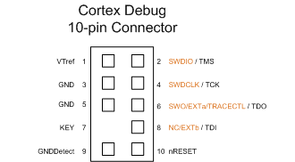
I went through the connections, although it doesn't seem that I can directly connect this to the nucleo-f722ze's st-link? Would I need to design my own link if I plan on using this connector.
I used
http://www.support.code-red-tech.com/CodeRedWiki/HardwareDebugConnections
which seems to cover the majority of the required connection pins and pullups.Thank you for all the help.
- Mark as New
- Bookmark
- Subscribe
- Mute
- Subscribe to RSS Feed
- Permalink
- Email to a Friend
- Report Inappropriate Content
2018-02-28 10:34 AM
The SWO, NRESET are at the green header AND connect to the TARGET processor on the Nucleo board.
The 10-pin header uses the same signals, it is just a standard rather than one pulled out of the air by ST.
Connects to an standalone ST-LINK, J-LINK or U-LINK, and there are adapters from the standard 20-pin header if that's too big for your application.
https://www.olimex.com/Products/ARM/JTAG/ARM-JTAG-20-10/
Up vote any posts that you find helpful, it shows what's working..
- Mark as New
- Bookmark
- Subscribe
- Mute
- Subscribe to RSS Feed
- Permalink
- Email to a Friend
- Report Inappropriate Content
2018-02-28 10:43 AM
10-pin SWD connector
Tag-Connect test points
Up vote any posts that you find helpful, it shows what's working..
- Mark as New
- Bookmark
- Subscribe
- Mute
- Subscribe to RSS Feed
- Permalink
- Email to a Friend
- Report Inappropriate Content
2018-02-28 11:08 AM
Hi
Turvey.Clive.002
Thank you for the detailed and informative response.
I completely understand the debugger connections now.
- Mark as New
- Bookmark
- Subscribe
- Mute
- Subscribe to RSS Feed
- Permalink
- Email to a Friend
- Report Inappropriate Content
2018-02-28 05:36 PM
Hi,
the RTC could be stable, and may not drift, its a matter of 'drift ppm'
the goal is to be accurate. long term.
How often would you want to adjust the clock ? if it was 5 minutes out, you would adjust it...
with the DS3232, it takes two years to be 5minutes out at worst.
the drift comes from the ppm of the crystal and the quality of the caps.
Generally you would put the board through the oven to solder everything as usual. then either immediately after the oven or after a several hours at 40/50C, you must coat the crystal 'capacitors' with conformal coating to lock out the humidity. Humidity will cause the capacitance to slightly change which effects the crystal frequency slightly.
32700000Hz would be great, but its a struggle to get that close. Hence I use the embedded crystal and caps in the DS3232 package for my industrial processes.
________________ Attachments : Terminal18.jpg : https://st--c.eu10.content.force.com/sfc/dist/version/download/?oid=00Db0000000YtG6&ids=0680X000006HxvV&d=%2Fa%2F0X0000000b2L%2FS0dm38DfA.g_pfqMu0BTJlDwjBlX6rKdYfj2agDnqs8&asPdf=falseT18Batt.jpg : https://st--c.eu10.content.force.com/sfc/dist/version/download/?oid=00Db0000000YtG6&ids=0680X000006HxsS&d=%2Fa%2F0X0000000b2K%2FSNJL3r_48X4JrDOoYY24W5A62avK5Aw44SzFH_dtLvU&asPdf=false- Mark as New
- Bookmark
- Subscribe
- Mute
- Subscribe to RSS Feed
- Permalink
- Email to a Friend
- Report Inappropriate Content
2018-03-01 01:37 AM
It looks like you have a pretty good handle on the issues. I would also go with the standard 10 pin debug socket, standards are standards after all. I found that as some peripherals are limited to 50MHz or 100MHz, using a 200MHz clock gave better performance than 216MHz as I could run the peripherals flat out. It doesn't affect your PCB of course.
- How to Add custom task along with Lorawan communication in STM32 MCUs Wireless
- STM32F405 ULPI USB3343 in STM32 MCUs products
- ADC not working at all - only output is "0" in STM32 MCUs Embedded software
- guidance for taking forward of custom hw using stm32h743 in STM32 MCUs Boards and hardware tools
- STM32F7 Ethernet (Without FreeRTOS): Not Working (No Ping) in STM32 MCUs products