- STMicroelectronics Community
- STM32 MCUs
- STM32 MCUs TouchGFX and GUI
- Re: FMC and SDRAM example
- Subscribe to RSS Feed
- Mark Topic as New
- Mark Topic as Read
- Float this Topic for Current User
- Bookmark
- Subscribe
- Mute
- Printer Friendly Page
FMC and SDRAM example
- Mark as New
- Bookmark
- Subscribe
- Mute
- Subscribe to RSS Feed
- Permalink
- Email to a Friend
- Report Inappropriate Content
2019-10-05 07:32 AM
Following up on my last question about the LTDC interface (That's now working) I'm working through the app note 4861.
Where for the LTDC interface there is a nice walkthrough on how to find the timing values there is nothing like that for the SDRAM selection. bummer.
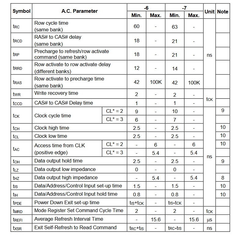
I have made a board with AS4C4M16SA for the SDRAM, datasheet here: https://www.alliancememory.com/wp-content/uploads/pdf/dram/64M-AS4C4M16SA-CI_v3.0_March%202015.pdf
The timing information is on page 20.
But the app note states that one can either use the CubeMX interface or use the BSP files.
it goes (lightly) over the BSP integration but don't mention the CubeMX at all.
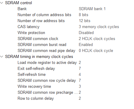
More specifically I am looking for a way to figure out the timing setup from the datasheet:

Also - since I'm running the TouchGFX integration I have a file called 'HW_Init.cpp' In the top there is a couple of definitions for the mode register.
I have changed this to reflect my new chip:
#define REFRESH_COUNT        1539

#define SDRAM_TIMEOUT                            ((uint32_t)0xFFFF)
#define SDRAM_MODEREG_BURST_LENGTH_1             ((uint16_t)0x0000)
#define SDRAM_MODEREG_BURST_LENGTH_2             ((uint16_t)0x0001)
#define SDRAM_MODEREG_BURST_LENGTH_4             ((uint16_t)0x0002)
#define SDRAM_MODEREG_BURST_LENGTH_8             ((uint16_t)0x0003)
#define SDRAM_MODEREG_BURST_TYPE_SEQUENTIAL      ((uint16_t)0x0007)
#define SDRAM_MODEREG_BURST_TYPE_INTERLEAVED     ((uint16_t)0x0008)
#define SDRAM_MODEREG_CAS_LATENCY_2              ((uint16_t)0x0020)
#define SDRAM_MODEREG_CAS_LATENCY_3              ((uint16_t)0x0030)
#define SDRAM_MODEREG_OPERATING_MODE_STANDARD    ((uint16_t)0x0000)
#define SDRAM_MODEREG_WRITEBURST_MODE_PROGRAMMED ((uint16_t)0x0000)
#define SDRAM_MODEREG_WRITEBURST_MODE_SINGLE     ((uint16_t)0x0200)
In the top there is a refresh count - I suspect that this value should also be changed - but to what?
Any help is appreciated!
Solved! Go to Solution.
Accepted Solutions
- Mark as New
- Bookmark
- Subscribe
- Mute
- Subscribe to RSS Feed
- Permalink
- Email to a Friend
- Report Inappropriate Content
2019-10-10 12:25 PM
A few last notes on this (because I always seem to forget a bit here and there)
I have made a video on my approach: https://www.youtube.com/watch?v=DNujNps9BWo
when you have verified that your display works, go on to the SDRAM. I suggest that you test it with the F7 repository example for the FMC interface.
I have found that you would need to change the following to get the SDRAM working (not necessarily in that order)
- check that the appropriate interrupts are enabled
- check the REFRESH_COUNT (mine magically 1292 - I'm not sure about that calculation though)
- set the 'defaultTask' stack size to 4096
- IMPORTANT: Increase the minimal heap size to something bigger than 4096*4 - I set mine to 32768 just to be sure.
- Mark as New
- Bookmark
- Subscribe
- Mute
- Subscribe to RSS Feed
- Permalink
- Email to a Friend
- Report Inappropriate Content
2019-10-05 07:51 AM
To work from datasheets you need to convert the cycle counts into nano-seconds, based on how you're clocking the interface, and then make sure these are adequate to meet the specifications. If CubeMX were more useful it would show you the cycle count AND ns speed.
You need to initiate a refresh at 64ms/4096 intervals, at bus clock
Up vote any posts that you find helpful, it shows what's working..
- Mark as New
- Bookmark
- Subscribe
- Mute
- Subscribe to RSS Feed
- Permalink
- Email to a Friend
- Report Inappropriate Content
2019-10-05 09:42 AM
well, you make it sound really simple :)
I would love to have a note or something to refer to while doing this.
I'm running at 200MHz, which should bring my interface to half or third of that - depening on what I choose in 'SDRAM common clock' - right?
that means either 100MHz or 66.6MHz. I'm going with 100MHz. that gives me a period of 10ns - easy to calculate with
refreshing time:
if I first find how many times 10ns can fit into 64ms - that is 6400000 times. I need to refresh 4096 times in that interval, so each 1562.5 cycle. got it. i'll just set it to 1562. (1041 for the 66.6MHz version)
Now I need to find the right numbers for all the other parameters - Most of them are minimum values so maybe I can just be on the safe side?
this is the timing values from the datasheet.
Load mode register to active delay:
I have no clue which number this is.. any clue??
Exit self-refresh delay:
datasheet says 'Trc +Tis' which is 60ns+1.5ns - if I set this to 7 I'm good (70ns)
Self-refresh time:
No idea..
SDRAM common row cycle delay:
is that the same as the Trc? if that is the case it could be set to 6..
Write recovery time:
datasheet says 2 cycles - that is 20ns.. I'll put 2 in CubeMX
SDRAM common row precharge delay:
looks like the Trp in the datasheet? setting to 2.
Row to column delay:
is that the Trcd in the datasheet? then it should be 2.
Does that seem about right?
- Mark as New
- Bookmark
- Subscribe
- Mute
- Subscribe to RSS Feed
- Permalink
- Email to a Friend
- Report Inappropriate Content
2019-10-05 10:20 AM
My expectation is the bus runs at 100 or 108 MHz for a typical F7 design, most of the SDRAM these days are good to 133, or 166 MHz. The slew rate set on the pins (SPEED) is typically 50 MHz, not 100 MHz (ie HIGH not VERY HIGH) as the signal paths are short and the bus load low.
Load mode register to active delay -> Mode Register Set Command Cycle Time
A better imagined automation tool would have an easily curated database of commonly available parts (with generic expression of parameters in cycles/time, so a close match can be selected), and an easy method to submit new devices for review and insertion into the database. Pretty low bandwidth task is executed properly.
Up vote any posts that you find helpful, it shows what's working..
- Mark as New
- Bookmark
- Subscribe
- Mute
- Subscribe to RSS Feed
- Permalink
- Email to a Friend
- Report Inappropriate Content
2019-10-06 05:10 AM
Yeah, I'm at 100MHz - just verified that I indeed get a clock pulse on the chip.
As far as your slew-rate comment I guess that is what I set in the MX setup - Maximum output speed? They are all set for 'very high'
It would indeed be nice with a tool to help select this. It's even easy to make that!
I would settle for less if I just had a guide to follow when doing this. isn't there any app note for this particular scenario??
What irks me is that I don't have any setting where I set the adress space for the SDRAM. I know it should start at 0xC0000000 - but where is that defined?
The only thing that I have so far is that the TouchGFX is configured to store the framebuffer with that starting adress - I'm only getting static on the screen. As per my last thread I know the screen is working so the only thing I have changed is the framebuffer pointer - that tells me that something is wrong with the SDRAM.. argh, this is frustrating!
- Mark as New
- Bookmark
- Subscribe
- Mute
- Subscribe to RSS Feed
- Permalink
- Email to a Friend
- Report Inappropriate Content
2019-10-07 11:45 AM
Okay, I solved this!
I'm not completely sure what I did so if there's interest I will try to retrace my steps.
I have fiddled around with the DMA2D and the framebuffers for quite some time and I knew that the screen was working.
I came across another thread on another subject that was using the examples from CubeMX to test a specific thing. I figured that I could do the same - so the FMC example for SDRAM was working straightaway. hmm.. I must be doing something wrong then.
I'm not sure I have the full picture (pun not intended) but I changed the heap size for the main task from 128(!!Seriously what the he**!?) to 4096 which is the amount that TouchGFX usually requires. I could see that my PSU was current limiting so I turned it a bit up (I'm at 210mA now - on the 3.3V side alone) and power cycled. Bingo - there is my touchGFX design..
I will most likely do a video on this in a few days - I can't be the only one struggling here???
- Mark as New
- Bookmark
- Subscribe
- Mute
- Subscribe to RSS Feed
- Permalink
- Email to a Friend
- Report Inappropriate Content
2019-10-10 12:25 PM
A few last notes on this (because I always seem to forget a bit here and there)
I have made a video on my approach: https://www.youtube.com/watch?v=DNujNps9BWo
when you have verified that your display works, go on to the SDRAM. I suggest that you test it with the F7 repository example for the FMC interface.
I have found that you would need to change the following to get the SDRAM working (not necessarily in that order)
- check that the appropriate interrupts are enabled
- check the REFRESH_COUNT (mine magically 1292 - I'm not sure about that calculation though)
- set the 'defaultTask' stack size to 4096
- IMPORTANT: Increase the minimal heap size to something bigger than 4096*4 - I set mine to 32768 just to be sure.
- OPENAMP STM32H745 memory problems in STM32 MCUs Embedded software
- H743 SDRAM memory failure in STM32 MCUs Embedded software
- SDRAM and a global struct. in STM32CubeIDE (MCUs)
- STM32H7S78-DK Template XIP external Ram setup bug found in STM32 MCUs Products
- Modal redraw question in STM32 MCUs TouchGFX and GUI
