- STMicroelectronics Community
- STM32 MCUs
- STM32 MCUs Products
- Re: Which internal memory address is memory mapped...
- Subscribe to RSS Feed
- Mark Topic as New
- Mark Topic as Read
- Float this Topic for Current User
- Bookmark
- Subscribe
- Mute
- Printer Friendly Page
Which internal memory address is memory mapped QUAD SPI mapped to?
- Mark as New
- Bookmark
- Subscribe
- Mute
- Subscribe to RSS Feed
- Permalink
- Email to a Friend
- Report Inappropriate Content
2018-03-11 12:33 PM
Hi, I want to setup my STM32F767 QUAD SPI peripheral to access an external NOR FLASH chip in memory mapped mode.
I can see from the STM32F76xxx reference manual how to set the QUADSPI->CCR register to set the FLASH memory command and frame format to configure it in memory mapped mode. Besides setting the CCR register, is there anything else I need to do, apart from the Timeout counter etc., to setup to operate it in memory mapped mode?
But I have not found anywhere in either the datasheet or the reference manual that defines which internal memory addresses are used to map the QUAD SPI peripheral to when it is operated in the memory mapped mode for reading from the FLASH chip.Does anyone know this?Thanks.- Mark as New
- Bookmark
- Subscribe
- Mute
- Subscribe to RSS Feed
- Permalink
- Email to a Friend
- Report Inappropriate Content
2018-03-11 3:02 PM
Examples I've seen all decode at 0x90000000
Up vote any posts that you find helpful, it shows what's working..
- Mark as New
- Bookmark
- Subscribe
- Mute
- Subscribe to RSS Feed
- Permalink
- Email to a Friend
- Report Inappropriate Content
2018-03-11 4:49 PM
Clive One wrote:
Examples I've seen all decode at 0x90000000
Indeed.

Might've been mentioned in RM, too...
JW
- Mark as New
- Bookmark
- Subscribe
- Mute
- Subscribe to RSS Feed
- Permalink
- Email to a Friend
- Report Inappropriate Content
2018-03-11 5:26 PM
My copy of RM0410 (Rev 3, Nov 2017, STM32F76xxx and STM32F77xxx) was less than illuminating on the topic. Closest to a mention was 0x90000000-0x9FFFFFFF was Bank 4 Reserved on the FMC
http://www.st.com/en/microcontrollers/stm32f767zi.html
Up vote any posts that you find helpful, it shows what's working..
- Mark as New
- Bookmark
- Subscribe
- Mute
- Subscribe to RSS Feed
- Permalink
- Email to a Friend
- Report Inappropriate Content
2018-03-11 5:30 PM
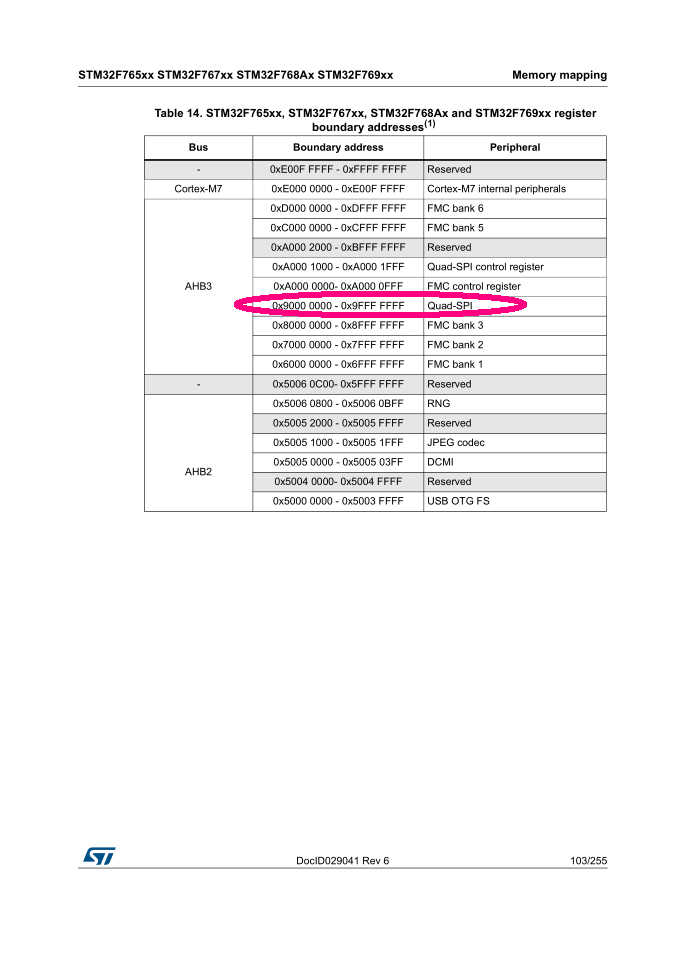
I didn't find it (directly) in RM either - the screenshot is from the DS...
Jan
- Mark as New
- Bookmark
- Subscribe
- Mute
- Subscribe to RSS Feed
- Permalink
- Email to a Friend
- Report Inappropriate Content
2018-03-11 5:33 PM
Yes I've now found some examples using address
0x90000000, and even found the following in the stm32f765xx.h device file
♯ define QSPI_BASE 0x90000000U /*!< Base address of : QSPI memories accessible over AXI */
However, there is no mention of this address in the reference manual RM04010 document.That manual does have the 'Table 1. STM32F76xxx and STM32F77xxx register boundary addresses', but that table, in that particular document, excludes the QSPI_BASE address. Obviously an omission on ST's part as some other reference manuals for other devices do include it.
But now looking at the datasheet, which usually is not very detailed, again, I do see the above Table 14.So problem, solved.Thanks folks.
- Mark as New
- Bookmark
- Subscribe
- Mute
- Subscribe to RSS Feed
- Permalink
- Email to a Friend
- Report Inappropriate Content
2018-03-11 5:41 PM
Yes, see it there, well that's just more depressing. Can we get an 'About the documentation' sub-forum?
Up vote any posts that you find helpful, it shows what's working..
- Mark as New
- Bookmark
- Subscribe
- Mute
- Subscribe to RSS Feed
- Permalink
- Email to a Friend
- Report Inappropriate Content
2018-03-13 9:37 AM
Hi,
Thank you for highlighting this issue
.This is noted and will be fixed in coming release of the reference manual.-Nesrine-
- I2C Not Working in STM32 MCUs Products
- Bricked two STM32WBA55 NUCLEO boards by flashing in CubeIDE (repeteable) in STM32 MCUs Products
- Fail to load images from the SD card in STM32 MCUs TouchGFX and GUI
- STM32F765 / Flash / Start address of bank 2 / problem with RM in STM32CubeProgrammer (MCUs)
- Using Internal Flash as Eprom at External Flash Application in STM32 MCUs Embedded software