- STMicroelectronics Community
- STM32 MCUs
- STM32 MCUs Products
- Re: Use ST_Link Programmer from Nucleo 64 F411RE B...
- Subscribe to RSS Feed
- Mark Topic as New
- Mark Topic as Read
- Float this Topic for Current User
- Bookmark
- Subscribe
- Mute
- Printer Friendly Page
Use ST_Link Programmer from Nucleo 64 F411RE Board to program a Stand Alone STM32F411RE Chips
- Mark as New
- Bookmark
- Subscribe
- Mute
- Subscribe to RSS Feed
- Permalink
- Email to a Friend
- Report Inappropriate Content
2017-07-13 6:41 AM
Hi, I have a ST_Link Programmer that was cut off from STM32F411RE Nucleo 64 Board (zero ohms resistors SB12, 13, 14, and 15 have been also removed). I have been use it to program other STM series Board with no problem.
Currently I am doing a project that is using STM32F411RE Nucleo 64 Board and I have a custom made PCB with STM32F411RE chips on it. I tried to use the same ST_Link Programmer to program the chips by connect the 8 pins from the programmer to the chips, but it does not work. The pins are connected the same as how I connect my programmer to the nucleo board.
When I connect the programmer to STM32F411RE Nucleo 64 Board:Programmer
- - - - - - - - - - - - - - - - - - - - - - - - - - - - -Board
Left Pin from JP1 (next to USB Power)- - - - - - -VDD (CN7-5) SWCLK (CN4-2)- - - - - - - - - - - - - - - - - - - - - - - - -PA14 (CN7-15) GND (CN4-3)- - - - - - - - - - - - - - - - - - - - - - - - - - -GND (CN7-8) SWDIO (CN4-4)- - - - - - - - - - - - - - - - - - - - - - - - -PA13 (CN7-13) NRST (CN4-5)- - - - - - - - - - - - - - - - - - - - - - - - - -NRST (CN7-14) SWO (CN4-6)- - - - - - - - - - - - - - - - - - - - - - - - - - -PB3 (CN10-31) TX (CN3-1)- - - - - - - - - - - - - - - - - - - - - - - - - - - - -PA3 - RX (CN10-37) RX (CN3-2)- - - - - - - - - - - - - - - - - - - - - - - - - - - - -PA2 - TX (CN10-35) With the connection above, I can program my Nucleo board with external ST-Link programmer that I cut off before. Everything works fine. And then I connected the same programmer to my STM32F411RE Chips with the same pins as following:Programmer
- - - - - - - - - - - - - - - - - - - - - - - - - - - -STM32F411RE MCU
Left Pin from JP1 (next to USB Power)- - - - - - - - - - - -VDD (Pin 19) SWCLK (CN4-2)- - - - - - - - - - - - - - - - - - - - - - - - - - - - - -PA14 (Pin 49) GND (CN4-3)- - - - - - - - - - - - - - - - - - - - - - - - - - - - - - - -VSS (Pin 18) SWDIO (CN4-4)- - - - - - - - - - - - - - - - - - - - - - - - - - - - - -PA13 (Pin 46) NRST (CN4-5)- - - - - - - - - - - - - - - - - - - - - - - - - - - - - - -NRST (Pin 7) SWO (CN4-6)- - - - - - - - - - - - - - - - - - - - - - - - - - - - - - - -PB3 (Pin 55) TX (CN3-1)- - - - - - - - - - - - - - - - - - - - - - - - - - - - - - - - - -PA3 - RX (Pin 17) RX (CN3-2)- - - - - - - - - - - - - - - - - - - - - - - - - - - - - - - - - -PA2 - TX (Pin 16) This time, when I connect the program to my computer, same storage disk (NODE_F411RE (D:)) has jumped out, however, in stead of usual two files ( DETAILS.TXT and MBED.HTM), there is one additional file called FAIL.TXT, and when I opened it out, it shows: The interface firmware FAILED to reset/halt the target MCU. I am not sure how to fixed this, if anyone can help, that would be appreciated. Thank you Note: this post was migrated and contained many threaded conversations, some content may be missing.- Mark as New
- Bookmark
- Subscribe
- Mute
- Subscribe to RSS Feed
- Permalink
- Email to a Friend
- Report Inappropriate Content
2017-07-13 7:50 AM
More indicative of VDDA/VREF+ not being powered. Also want capacitors on VCAP pin(s).
Up vote any posts that you find helpful, it shows what's working..
- Mark as New
- Bookmark
- Subscribe
- Mute
- Subscribe to RSS Feed
- Permalink
- Email to a Friend
- Report Inappropriate Content
2017-07-13 10:18 AM
Hi, thanks for the reply. So do I connect Left Pin from JP1 (power) to VDDA/VREF+? What is VCAP pin(s)? and what size of capacitors that I should use? Thank you.
- Mark as New
- Bookmark
- Subscribe
- Mute
- Subscribe to RSS Feed
- Permalink
- Email to a Friend
- Report Inappropriate Content
2017-07-13 10:46 AM
There's a manual for the part that's worth reviewing
Single VCAP pin (30) would need a 4u7F, it's the bulk capacitor for the 1.25V regulator powering the core. The VDDA/VREF+ powers the analogue circuitry (so POR and PLL/VCO as I recall), no power there device held in reset indefinitely.
Up vote any posts that you find helpful, it shows what's working..
- Mark as New
- Bookmark
- Subscribe
- Mute
- Subscribe to RSS Feed
- Permalink
- Email to a Friend
- Report Inappropriate Content
2017-07-13 11:34 AM
Thanks! I will try it tomorrow by adding power to VDDA/VREF+ and add a capacitor from VCAP to ground.
- Mark as New
- Bookmark
- Subscribe
- Mute
- Subscribe to RSS Feed
- Permalink
- Email to a Friend
- Report Inappropriate Content
2017-07-14 10:11 AM
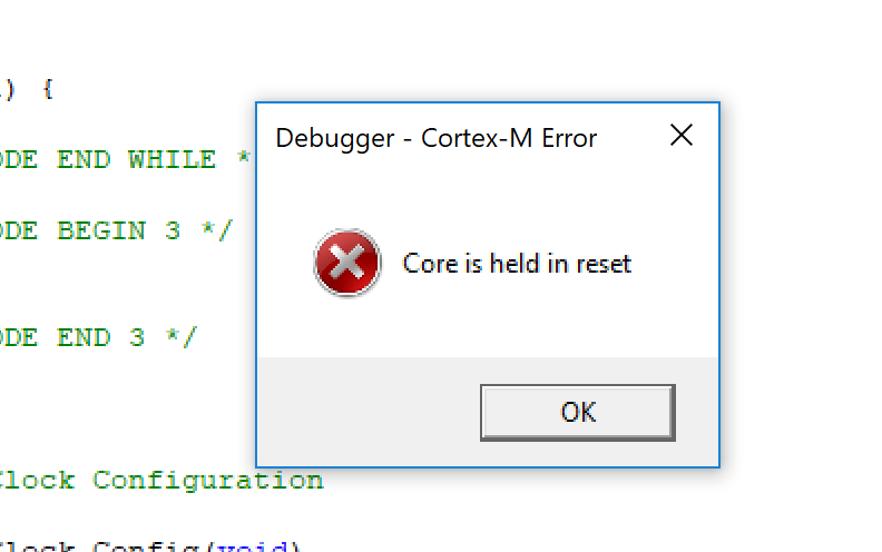
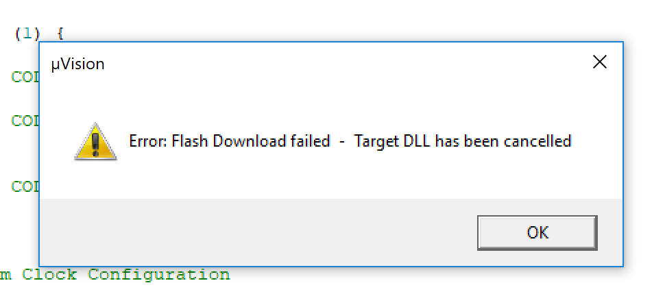
Hi Clive One, I have tried what you said today, by adding power to VDDA/VERF+, The FAIL.TXT has gone, however, when I upload code from Keil (I am using STM32Cube MX combined with Keil to program the MCU), it returned with Core is held in reset. And I am not able to upload any code.


And then I tried to add a 4.7uF capacitor between VCAP (Pin 30) and GND, as soon as added it, the FAIL.TXT Jumps out again, original problem has come up again.
Is there anything else I've missed? I will read through the document that you recommended, but if you have any suggestions, that would be great.
PS. I have checked my custom made PCB, before I connect the programmer to the PCB, the following connection has already made:
the NRST (PIN 7) of MCU is connected to GND with BOOT0 (PIN 60)
OSC_IN (PIN 5) and OSC_OUT (PIN 6) are also connected to GND
VDDA/VERF+ (Pin 13) and VBAT (Pin 1) are connected to 3.6V
VSSA/VREF- (Pin 12) is connected to 100uF capacitor and the capacitor is then connected to GND.
Thank you!
- Mark as New
- Bookmark
- Subscribe
- Mute
- Subscribe to RSS Feed
- Permalink
- Email to a Friend
- Report Inappropriate Content
2017-07-14 10:56 AM
VSSA should connect to GROUND
Check voltage levels on VCAP pin and NRST pin.
Up vote any posts that you find helpful, it shows what's working..
- Mark as New
- Bookmark
- Subscribe
- Mute
- Subscribe to RSS Feed
- Permalink
- Email to a Friend
- Report Inappropriate Content
2017-07-14 11:34 PM
I don't have the PCB with me at the moment, but as I remembered, the VSSA is connected to Ground through a 100uF capacitor, I am not sure if the capacitor will make any difference.
Not sure about the voltage level on VCAP pin. However, the NRST and BOOT0 are connected together to the Ground, so I think there is no voltage level on NRST pin.
- Mark as New
- Bookmark
- Subscribe
- Mute
- Subscribe to RSS Feed
- Permalink
- Email to a Friend
- Report Inappropriate Content
2017-07-14 11:48 PM
VSSA should not 'go through' the capacitor to ground, it should be at ground potential.
NRST should not be connected to ground permanently.
If you hold NRST low the device is not going to function, because you're 'Holding the Core in Reset'
Perhaps you have someone with some electronics experience/qualifications who can help you
Up vote any posts that you find helpful, it shows what's working..
- Mark as New
- Bookmark
- Subscribe
- Mute
- Subscribe to RSS Feed
- Permalink
- Email to a Friend
- Report Inappropriate Content
2017-07-14 11:59 PM
Thanks a lot, that make sense to me. The PCB was designed by my friend, however he recently just left this project and I am taking his job over, I am not sure why he made those connections, I will try to get myself familiar with the document through the weekend and try it again on Monday.
- STM32Cube Programmer with STM32L522 bootloader run after programming in STM32 MCUs Products
- Output log showing HWrst mode while it's connected over DFU mode in STM32CubeProgrammer (MCUs)
- STlink different pinout information in STM32 MCUs Boards and hardware tools
- How to verify the correctness of the MCU internal program in Stm32cube programmer without changing RDP in STM32CubeProgrammer (MCUs)
- Stm32 stopped working after soldering components in STM32 MCUs Products