- STMicroelectronics Community
- STM32 MCUs
- STM32 MCUs Products
- Re: STM32 use SPI implement SWD?
- Subscribe to RSS Feed
- Mark Topic as New
- Mark Topic as Read
- Float this Topic for Current User
- Bookmark
- Subscribe
- Mute
- Printer Friendly Page
STM32 use SPI implement SWD?
- Mark as New
- Bookmark
- Subscribe
- Mute
- Subscribe to RSS Feed
- Permalink
- Email to a Friend
- Report Inappropriate Content
2019-12-06 12:53 AM
I want to use SPI implement SWD protocol. Found this one enter link description here
Is there any advice you can provide detail?
Have a nice day
Solved! Go to Solution.
- Labels:
-
SPI
Accepted Solutions
- Mark as New
- Bookmark
- Subscribe
- Mute
- Subscribe to RSS Feed
- Permalink
- Email to a Friend
- Report Inappropriate Content
2019-12-07 09:13 AM
And what speed do you expect with bit banging with a low power sysclk of 48MHz?
Here we are at 12/24 MHz. If SYSCLK is pll cranked up to 96 or 144 MHz....
One more point to look at it: When we rely on SPI FIFO, other interrupts such as USB can partially kick in while waiting at less penalty.
As Debugger is a USB to SWD bridge, it wouldn't look like using SPI being a regression.
There are some new SPI IP such as the one with STM32L4R5 supposely offering a 3 wire interface (supposely avoiding to short miso and mosi outside), with this exercise, discovered its functionality was inadequate as its behaviour seems like the half duplex SPI (with slippery SCKs)
for data deciphering, it's more like using wait dead time to time slice the computation avoiding to do all at the end. Here the data is done in chunks.
In general a HW assist is desireable to reduce SW workload and critical timings.
Anyway, I guess the answer has been provided to the question. Free speech always welcome. =)
- Mark as New
- Bookmark
- Subscribe
- Mute
- Subscribe to RSS Feed
- Permalink
- Email to a Friend
- Report Inappropriate Content
2019-12-06 02:40 AM
You need to switch direction and length quite often. And normaly you run SWD at some high frequency. So carefully think what you gain of using SPI with regard to processor cycles vs bitbanging with reduced complexity.
It is also a pity the the minimum SPI length is 4 and not one, so Jtag with its setting of TMS in the last cycle is also quite hard. Bl*ck M*g*c Debug probe uses pure bitbanging.
- Mark as New
- Bookmark
- Subscribe
- Mute
- Subscribe to RSS Feed
- Permalink
- Email to a Friend
- Report Inappropriate Content
2019-12-06 02:53 AM
It would be nice to the the implementation in Stlink /StlinkV3...
- Mark as New
- Bookmark
- Subscribe
- Mute
- Subscribe to RSS Feed
- Permalink
- Email to a Friend
- Report Inappropriate Content
2019-12-06 02:54 AM
Thank you for your advice
How can I switch spi to receive 3 bit with the ack?
I used gpio to implement swd, but I want to try more faster about spi
- Mark as New
- Bookmark
- Subscribe
- Mute
- Subscribe to RSS Feed
- Permalink
- Email to a Friend
- Report Inappropriate Content
2019-12-06 02:57 AM
I also think it is more better than myself, I will try it
Have a nice holiday
- Mark as New
- Bookmark
- Subscribe
- Mute
- Subscribe to RSS Feed
- Permalink
- Email to a Friend
- Report Inappropriate Content
2019-12-06 04:01 AM
>How can I switch spi to receive 3 bit with the ack?
Receive 4 bits including the turn-around bit
- Mark as New
- Bookmark
- Subscribe
- Mute
- Subscribe to RSS Feed
- Permalink
- Email to a Friend
- Report Inappropriate Content
2019-12-06 04:41 AM
You can do swd with spi if you use spi with fifo and variable bit size. At least no need to manipulate the gpio except disabling mosi when reading back data. No bitbang needed. The tricm is to group the turnaround bits and see 5 bit when you see 3 and slice the 32 bit with parity in something like 8 8 9 bits.
- Mark as New
- Bookmark
- Subscribe
- Mute
- Subscribe to RSS Feed
- Permalink
- Email to a Friend
- Report Inappropriate Content
2019-12-06 11:20 AM
Here some code extract to give you directions:
I used this link to get baseline: https://www.cnblogs.com/shangdawei/p/4753040.html
You will short MISO and MOSI outside. Here is STM32L4R5 in BGA132 @ 48MHz SYSCLK (low power) with 12 MHz SPI
IO_Pin_t SWDCLK_PIN = { // PB3 = SCK3
  GPIOB,   { GPIO_PIN_3,  GPIO_MODE_AF_PP,     GPIO_PULLDOWN,  GPIO_SPEED_FREQ_VERY_HIGH, 6  }, // SPI3_AF
};

IO_Pin_t SWDO_PIN = {  // PB5 = MOSI3 (bidir)
  GPIOB,   { GPIO_PIN_5,  GPIO_MODE_AF_PP,     GPIO_PULLDOWN,  GPIO_SPEED_FREQ_HIGH, 6  }, // SPI3_AF
};

IO_Pin_t SWDI_PIN = { // PB4 = MISO3 (no use)
  GPIOB,   { GPIO_PIN_4,  GPIO_MODE_AF_PP,     GPIO_NOPULL,  GPIO_SPEED_FREQ_HIGH, 6  }, // SPI3_AF
};
Next, some handy functions you will need:
uint8_t NibbleBitCounter[16] = {
  0, // 0000
  1, // 0001
  1, // 0010
  0, // 0011
  1, // 0100
  0, // 0101
  0, // 0110
  1, // 0111
 //-------- symmetrical
  1, // 1000
  0, // 1001
  0, // 1010
  1, // 1011
  0, // 1100
  1, // 1101
  1, // 1110
  0  // 1111
};

//==== here we directly control SPI with FIFO, IP version 2
// you change the speed between read and write due to setup time difference.
// don't change the clock polarity dynamically, it's a side effect generator.
void SWD_SetSPICR1Normal(void);
void SWD_SetSPICR1Normal(void) {
  SPI3->CR1 = ((SPI3->CR1)&0xFFC7)| (0<<3); // 24MHz
}

void SWD_SetSPICR1Slower(void);
void SWD_SetSPICR1Slower(void) {
  SPI3->CR1 = ((SPI3->CR1)&0xFFC7)| (1<<3);  // 12 MHz
}

void SWD_InitSPI(void) {

IO_PinConfigure(&SWDCLK_PIN); // PB3 = SCK3
IO_PinConfigure(&SWDO_PIN);  // PB5 = MOSI3 (bidir)
IO_PinConfigure(&SWDI_PIN); // PB4 = MISO3 (no use)

  __HAL_RCC_SPI3_CLK_ENABLE();  // Enable SPI2 clock
  SPI3->CR1 =  0//     (1<<15)  // bidir = 1
                //  | (1<<14)  // TX mode, output enabled
                  | (1<<9) // SSM=1
                  | (1<<8)
                  | (1<<7)   // LSB first
                  | (0<<3)   // prescaler div1 = 24 MHz
                  | (1<<2)      // master mode
                  | (0<<1) // SCK is low when idle
                  | (1<<0); // the second clock edge is the data capture's


  SPI3->CR2 =       (0<<12) // RXNE when 8+bit in FIFO
              |     (7<<8); // 8 bit mode (n-1)

  SPI3->CR1 |= (1<<6); // SPI enable

  // now let's look at the generated signals...
}

void SWD_WaitIdle(void);
void SWD_WaitIdle(void) {
  while(SPI3->SR & 1<<7); // wait while BUSY (transaction complete)
}
void SWD_Wait_u16(void);
void SWD_Wait_u16(void) {
  while(SPI3->SR & (1<<12)); // while the FIFO can't digest 16 bit
}

void SWD_RxMode(void);
void SWD_RxMode(void) {
  uint32_t moder = GPIOB->MODER;
  moder = moder & ~(3<<10); // 0 = digital input
  GPIOB->MODER = moder;
//  SPI3->CR1 |= ~(1<<14); // TX mode
}

void SWD_TxMode(void);
void SWD_TxMode(void) {
  uint32_t moder = GPIOB->MODER;
  moder = moder | (2<<10); // 2 = output AF
  GPIOB->MODER = moder;
//  SPI3->CR1 &= ~(1<<14); // RX mode
}

void SWD_SetBits(uint8_t bits);
void SWD_SetBits(uint8_t bits) {

  uint16_t r;
  r = SPI3->CR2;
  r &= ~(15<<8);
  r |= (bits-1)<<8; // go to n-1 bit mode
  SPI3->CR2 = r;
}

void FlushRxFifo(void);
void FlushRxFifo(void) {
  SWD.flushed = *((__IO uint8_t *)&SPI3->DR);
  SWD.flushed = *((__IO uint8_t *)&SPI3->DR);
  SWD.flushed = *((__IO uint8_t *)&SPI3->DR);
  SWD.flushed = *((__IO uint8_t *)&SPI3->DR);
}

void SWD_SwitchSPI(uint16_t sequence) {

  SWD_WaitIdle();//SWD_Wait_u16();

  // send the resynch
  *(__IO uint16_t *)&SPI3->DR = 0xFFFF; // 16 bit
  *(__IO uint16_t *)&SPI3->DR = 0xFFFF; // 32 bit
  SWD_Wait_u16();//SWD_WaitIdle();
  *(__IO uint16_t *)&SPI3->DR = 0xFFFF; // 48 bit
  SWD_Wait_u16();//
  *(__IO uint8_t *)&SPI3->DR = 0xFF; // 56 bit
  SWD_Wait_u16();//SWD_WaitIdle();
  *(__IO uint16_t *)&SPI3->DR = sequence;
  SWD_WaitIdle();
  FlushRxFifo();
}

void SWD_SyncSPI(void) {

  SWD_WaitIdle();
  // send the resynch
  *(__IO uint16_t *)&SPI3->DR = 0xFFFF; // 16 bit
  *(__IO uint16_t *)&SPI3->DR = 0xFFFF; // 32 bit
  SWD_Wait_u16();//SWD_WaitIdle();
  *(__IO uint16_t *)&SPI3->DR = 0xFFFF; // 48 bit
  SWD_Wait_u16();//
  *(__IO uint8_t *)&SPI3->DR = 0x3F; // 56 bit with 2 idle bits
  SWD_WaitIdle();
  FlushRxFifo();
}- Mark as New
- Bookmark
- Subscribe
- Mute
- Subscribe to RSS Feed
- Permalink
- Email to a Friend
- Report Inappropriate Content
2019-12-06 11:21 AM
Part 2 (this forum can't put all in one answer...)
Then you get something like this:
void SWD_Read(uint8_t cmd, uint32_t* pdata32) {

  uint32_t readback;
  uint8_t Regs[7];

  SWD_WaitIdle();
  FlushRxFifo();

  *(__IO uint8_t *)&SPI3->DR = cmd; // CMD transmit 8 bit

  SWD_WaitIdle();

  SWD_RxMode();
  SWD_SetSPICR1Slower();
  SWD_SetBits(5);
   *(__IO uint8_t *)&SPI3->DR = 0x99; // move 5 bits
  SWD_WaitIdle();
  readback = *((__IO uint16_t *)&SPI3->DR); // read past 8 + 5 bit
  SWD_SetSPICR1Normal();
  SWD_SetBits(8);
  Regs[0] = readback & 0xFF;
  readback >>= 8;
  Regs[1] = readback;
  SWD.Ack = (readback & 0x0E)>>1;
  SWD.du32 = (readback & 0x10)>>4;
  SWD.bitsum = SWD.du32;

  if(SWD.Ack!=0x01) { // NOK
    // error and abort
    SWD_TxMode();
    return;
  };

  // OK, so now we read the leftover bits (lsb is captured already)
  *(__IO uint8_t *)&SPI3->DR = 0x99; // move 8 bit LSB
  *(__IO uint8_t *)&SPI3->DR = 0x99; // move 8 not
  *(__IO uint8_t *)&SPI3->DR = 0x99; // move 8 bit
  SWD_WaitIdle();
  Regs[2] = *((__IO uint8_t *)&SPI3->DR);
  Regs[3] = *((__IO uint8_t *)&SPI3->DR);
  Regs[4] = *((__IO uint8_t *)&SPI3->DR);
  SWD_SetBits(9);
  *(__IO uint16_t *)&SPI3->DR = 0x9999; // move 8+1 bits

  SWD.temp32 = Regs[2];
  SWD.du32 |= (SWD.temp32<<1);
  SWD.bitsum ^= NibbleBitCounter[(SWD.temp32>>0) & 0x0F];
  SWD.bitsum ^= NibbleBitCounter[(SWD.temp32>>4) & 0x0F];
  SWD.temp32 = Regs[3];
  SWD.du32 |= (SWD.temp32<<9);
  SWD.bitsum ^= NibbleBitCounter[(SWD.temp32>>0) & 0x0F];
  SWD.bitsum ^= NibbleBitCounter[(SWD.temp32>>4) & 0x0F];
  SWD.temp32 = Regs[4];
  SWD.du32 |= (SWD.temp32<<17);
  SWD.bitsum ^= NibbleBitCounter[(SWD.temp32>>0) & 0x0F];
  SWD.bitsum ^= NibbleBitCounter[(SWD.temp32>>4) & 0x0F];

  SWD_WaitIdle();
  Regs[5] = *((__IO uint8_t *)&SPI3->DR);
  Regs[6] = *((__IO uint8_t *)&SPI3->DR); // turnaround bit included

  SWD_SetBits(8);
  SWD_TxMode();
  // we rebuild all decoded values
  SWD.temp32 = Regs[5];
  SWD.du32 |= ((SWD.temp32&0x7F)<<25);
  SWD.bitsum ^= NibbleBitCounter[(SWD.temp32>>0) & 0x0F];
  SWD.bitsum ^= NibbleBitCounter[(SWD.temp32>>4) & 0x0F];   // includes parity bit

  SWD.parity = (SWD.temp32 & 0x80)>>7;// optional
  // calculate the parity bit
  //if((SWD.bitsum)/*||(SWD.du32!=0x2BA01477)*/)
  //  NOPs(1);

  *pdata32 = SWD.du32;
}

SWD_CmdStatusT SWD_WriteDAPRegSPI(uint8_t cmd, uint32_t data) {

  SWD.Retrials = 0;
  do { // send the command until ACK or WAIT with timeout

    SWD_Write(cmd, data);

  }  while(     (  (SWD.Ack == 0x02) )
                &&   ((SWD.Retrials++)<30)
             );

  if(SWD.Retrials>SWD.WriteCmdWaitMax)
    SWD.WriteCmdWaitMax = SWD.Retrials; // keep track of the max nb of retrials for a write

  switch(SWD.Ack) { // analyse the command's answer
  case 0x01: // OK
    SWD.CmdStatus = SWD_CMD_OK;
    break;
  case 0x02: // TIMEOUT
    SWD.CmdStatus = SWD_CMD_WAIT;
    break;
  case 0x04: // FAULT
    SWD.CmdStatus = SWD_CMD_FAULT;
    break;
  default: // other error
    SWD.CmdStatus = SWD_CMD_ERROR;
  }

  return SWD.CmdStatus;

}

void SWD_Write(uint8_t cmd, uint32_t data32) {

  uint32_t readback;
  SWD_WaitIdle();
  FlushRxFifo();

  *(__IO uint8_t *)&SPI3->DR = cmd; // Transmit CMD 8 bit

  SWD_WaitIdle();

  SWD_RxMode();
  SWD_SetSPICR1Slower();
  SWD_SetBits(5);

  *(__IO uint8_t *)&SPI3->DR = 0x99; // send 5 bits = Tn ACK Tn

  SWD_WaitIdle();
  readback = *((__IO uint16_t *)&SPI3->DR); // read the answer
  SWD_SetSPICR1Normal();
  SWD_SetBits(8);
  SWD_TxMode();

//  SWD.Regs[0] = readback & 0xFF;
//  SWD.Regs[1] = readback >> 8;
  SWD.Ack = (readback >>9) & 0x07;

  if(SWD.Ack!=0x01) { // NOK
    NOPs(1);
    // error and abort
    return;
  };

  // OK, so now we read the leftover bits (lsb is captured already)
  *(__IO uint8_t *)&SPI3->DR = (data32 >>0) & 0xFF; // send 8 bit (hopefully)
  *(__IO uint8_t *)&SPI3->DR = (data32 >>8) & 0xFF; // send 8 bit (hopefully)
  *(__IO uint8_t *)&SPI3->DR = (data32 >>16) & 0xFF; // send 8 bit (hopefully)
  // Here we prepare the data to transmit Regs[2..3..4..5]
  // LSB to MSB
  SWD.temp32 = data32;//SWD.Regs[2] | (SWD.Regs[3]<<8) | (SWD.Regs[4]<<16) | (SWD.Regs[5]<<24);
  SWD.bitsum  = NibbleBitCounter[(data32>>0) & 0x0F];
  SWD.bitsum ^= NibbleBitCounter[(data32>>4) & 0x0F];
  SWD.bitsum ^= NibbleBitCounter[(data32>>8) & 0x0F];
  SWD.bitsum ^= NibbleBitCounter[(data32>>12) & 0x0F];
  SWD.bitsum ^= NibbleBitCounter[(data32>>16) & 0x0F];
  SWD.bitsum ^= NibbleBitCounter[(data32>>20) & 0x0F];
  SWD.bitsum ^= NibbleBitCounter[(data32>>24) & 0x0F];
  SWD.bitsum ^= NibbleBitCounter[(data32>>28) & 0x0F];
  SWD.parity = SWD.bitsum;
  SWD.temp32 = ((data32 >>24) & 0xFF ) |((SWD.bitsum & 0x01)<<8); // parity bit

  SWD_WaitIdle();
  SWD_SetBits(9);

  *(__IO uint16_t *)&SPI3->DR = SWD.temp32; // send 9 bit (hopefully)
  SWD_WaitIdle();
  FlushRxFifo();
  SWD_SetBits(8);
}
This is a fun experiment, you can start/stop/reset the core, read/write internal RAM.
SPI speed tuning, rugged test, higher level error management has not been done.
Consider this as pseudo code to shrink dev time only.
- Mark as New
- Bookmark
- Subscribe
- Mute
- Subscribe to RSS Feed
- Permalink
- Email to a Friend
- Report Inappropriate Content
2019-12-06 11:37 AM
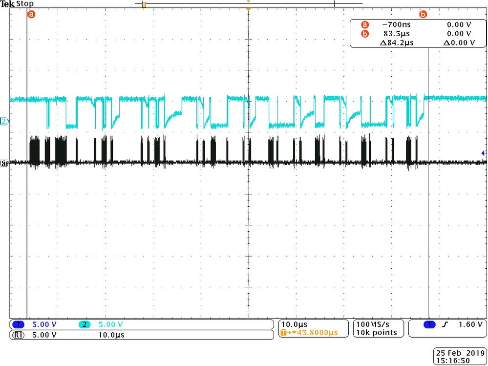
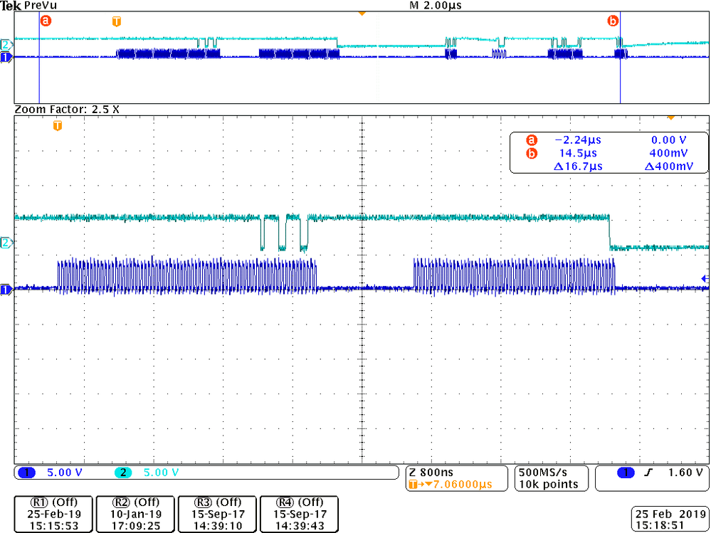
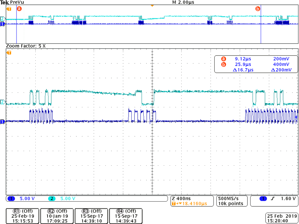
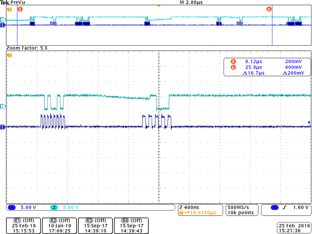
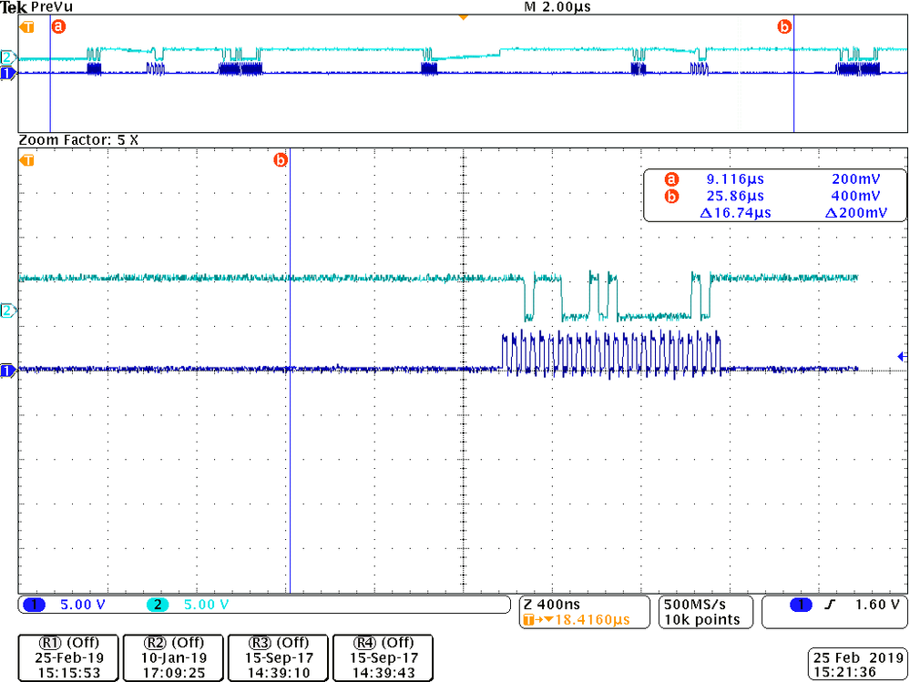
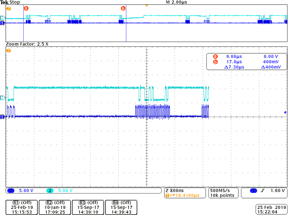
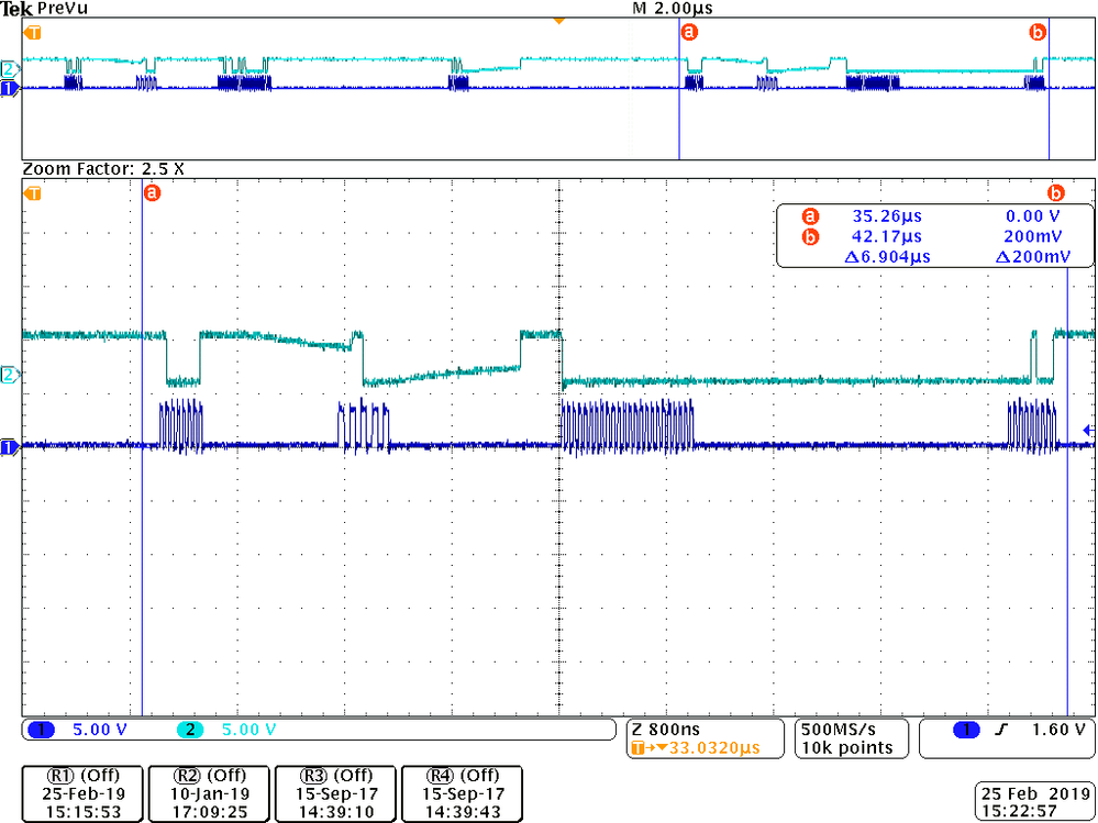
Some pictures
So to have a even fast communication, the SPI should have a special mode where the data register is split in MSB = bit length with R/W, LSB = data bits
Then the delay between packets could be minimized and average speed improved further. A true 3 wire interface would save 1 GPIO unless voltage shifting required outside.


