- STMicroelectronics Community
- STM32 MCUs
- STM32 MCUs Products
- Re: L476 Problems getting the FMC working with SSD...
- Subscribe to RSS Feed
- Mark Topic as New
- Mark Topic as Read
- Float this Topic for Current User
- Bookmark
- Subscribe
- Mute
- Printer Friendly Page
L476 Problems getting the FMC working with SSD1963
- Mark as New
- Bookmark
- Subscribe
- Mute
- Subscribe to RSS Feed
- Permalink
- Email to a Friend
- Report Inappropriate Content
2017-03-08 03:15 PM
We are having problems trying to make a 320x240 LCD Color Display working on the L476 FMC Peripheral. The LCD uses the SSD1963 chipset. We have hooked the SSD1963 up to the FMC like an 8080 SRAM device using the parallel 16-bit data bus and 1 Data Address bit to communicate. For some reason, we can't seem to get the FMC to duplicate the waveforms on the SSD1963 specification.....A0 address line will not stay asserted during data write, and the CS line is way off from any Data Access signal. Could someone point us to what is going on? BTW, we are using the STMCubeMX HAL drivers for our project.
Let me also mention that we would be glad to pay someone who has gotten the FMC working with the SSD1963 as well. Just E-mail me at
mailto:rasmusjc@gmail.com,
and I'll forward you to our manager.Thanks,
--James Rasmussen
#l476-fmc-lcd-ssd1963- Labels:
-
FMC-FSMC
- Mark as New
- Bookmark
- Subscribe
- Mute
- Subscribe to RSS Feed
- Permalink
- Email to a Friend
- Report Inappropriate Content
2017-03-08 03:48 PM
Post the captured waveforms and the content of relevant FMC and GPIO registers.
You might also want to contact the guy from en.radzio.dxp.pl/ssd1963/ .
JW
- Mark as New
- Bookmark
- Subscribe
- Mute
- Subscribe to RSS Feed
- Permalink
- Email to a Friend
- Report Inappropriate Content
2017-03-09 09:15 AM
Thanks for the replay and I'll will contact the person you mention above...
Meanwhile, I found this post from someone trying the ssd1963 on the FMC on an F7. He has nicely supplied the same waveforms I am seeing when using FMC vs. GPIO. Please see the forum posting here:
- Mark as New
- Bookmark
- Subscribe
- Mute
- Subscribe to RSS Feed
- Permalink
- Email to a Friend
- Report Inappropriate Content
2017-03-09 10:51 AM
>the guy from en.radzio.dxp.pl/ssd1963/
created a nice and well designed SSD1963 driver, but the driver uses GPIOs, not FM(S)C/i8080
- Mark as New
- Bookmark
- Subscribe
- Mute
- Subscribe to RSS Feed
- Permalink
- Email to a Friend
- Report Inappropriate Content
2017-03-21 11:32 AM
After working the problem, I've found that the NE1/NE3 lines on the FMC do not generate a sufficient chip select signal for the SSD1963 interface chip used in our Riverdi TFT 320x240 Color Display (Did not matter if it was Mode A, B, or D for an SRAM on the FMC, and the FMC was configured as NOR/SAM Bank 1). I had to map the CS pin as a GPIO Output, and permanently set it low, then the FMC worked as expected with the display.
I have seen nothing on how to further manipulate the NE1/NE3 signal timing under FMC Control. Does anyone have any idea how to do this?
Thanks.
- Mark as New
- Bookmark
- Subscribe
- Mute
- Subscribe to RSS Feed
- Permalink
- Email to a Friend
- Report Inappropriate Content
2017-03-22 02:36 AM
Have you alredy got a new datasheet for the SSD1963 as I've said in the parallel thread? What are your findings exactly?
JW
- Mark as New
- Bookmark
- Subscribe
- Mute
- Subscribe to RSS Feed
- Permalink
- Email to a Friend
- Report Inappropriate Content
2017-03-22 07:37 AM
The latest actual datasheet that I could find for the SSD1963 is Rev1.6, Aug. 2012, which is the version I have had even before I made the initial post.
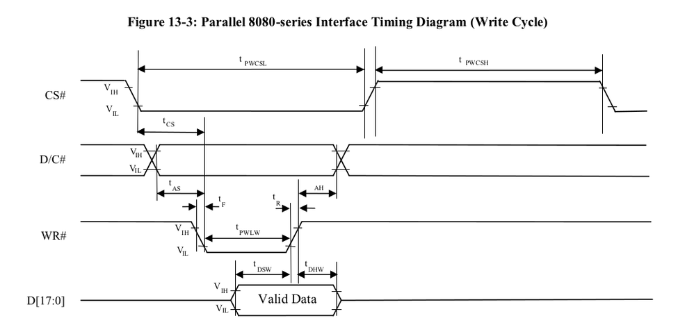
I my first reply I asked you to provide *captured* waveforms; you pointed me to that parallel post where a screenshot from an old version of the DS was posted, with waveforms completely out of normal i8080 sequence.
I still would like to see the captured waveforms and register setup, so that we could ccmpare them to the requirements put in DS.
JW
- Mark as New
- Bookmark
- Subscribe
- Mute
- Subscribe to RSS Feed
- Permalink
- Email to a Friend
- Report Inappropriate Content
2017-03-22 08:09 AM
 Here is what I get from my logic Analyzer from the Eval Board (Note: A0 drives the D/C# line and the Data Lines are not shown because I can't find an access to them even on the Eval Board) CS is driven by NE3/NE1:
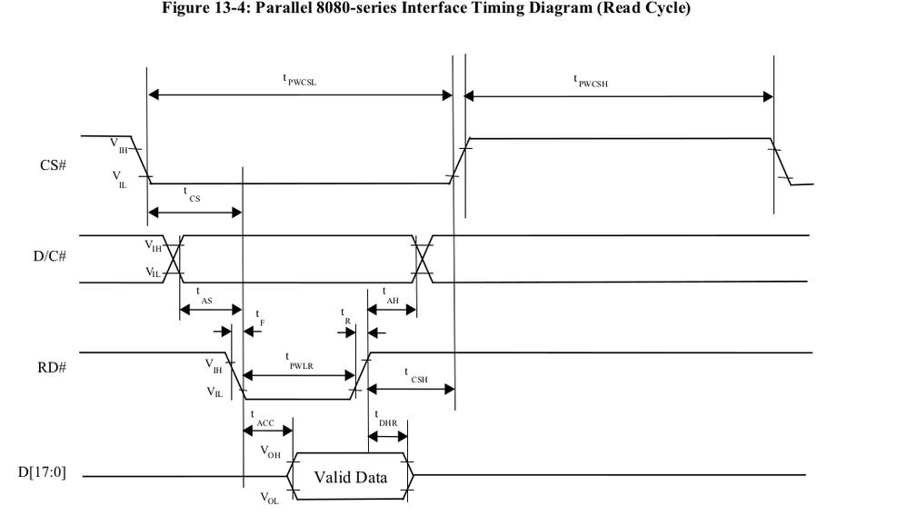
  Below is the SSD1963 Read Timing Diagram from the SSD1963 Spec (Pg. 84):
And Here is what the Read Cycle on the Eval Board's FMC looks like on my Logic Analyzer: 
- Mark as New
- Bookmark
- Subscribe
- Mute
- Subscribe to RSS Feed
- Permalink
- Email to a Friend
- Report Inappropriate Content
2017-03-22 08:19 AM
Yes, I have searched for the latest revisions. The latest actual datasheet that I could find for the SSD1963 is Rev1.6, Aug. 2012, which is the version I have had even before I made the initial post.
I have gotten the SSD1963 interfaced display working, but I had to make the CS pin like a permanent GPIO ground, instead of letting it being controlled by the FMC. If I let the FMC control the CS, then the display misses some of the read/write transactions to it which affect what is put on the display, and the LCD setup. My guess is that the CS timing is too tight for the LCD Display. Is there a way to even adjust the CS timing relative to the Read/Write timing transactions? I haven't seen anything that says this can be done. I need the CS to go low about 4 HCLKs before the Address Bit is put on the bus, and have it stay low until after the trailing edge of the RD or WR signal.- Mark as New
- Bookmark
- Subscribe
- Mute
- Subscribe to RSS Feed
- Permalink
- Email to a Friend
- Report Inappropriate Content
2017-03-22 09:34 AM
You've posted the same picture twice.
You did not post the content of relevant FSMC registers.
In the 'L476 there's no FMC according to my copy of RM0351.
According to UM1855, some of the data lines are brough out to RM6/RM7. Btw, how did you connect the display physically?
There's also something terribly wrong: the write pulse should end (rising edge) one HCLK before CS (rising edge). What's the HCLK frequency?
Also the fact that CS goes low soon after that write is suspicious, I see no reason for that.
Set the analyzer to 500MHz otherwise the granularity of 5ns at 200MHz might cause some edges to appear to overlap.
JW
- N6 VS Code launch.json for debugging in STM32 VSCode extension (MCUs)
- File Hierarchy problem in MTP in STM32 MCUs Embedded software
- Static library creation and impelementation to another empty project in STM32CubeIDE (MCUs)
- SVD fixes of FLASH registers for F2, F4 and F7 MCU in STM32 MCUs Embedded software
- SDIO, USB Mass Storage, and Mac in STM32 MCUs Embedded software