- STMicroelectronics Community
- STM32 MCUs
- STM32 MCUs Products
- Re: How to interface 1Gbit Parallel NOR Flash with...
- Subscribe to RSS Feed
- Mark Topic as New
- Mark Topic as Read
- Float this Topic for Current User
- Bookmark
- Subscribe
- Mute
- Printer Friendly Page
How to interface 1Gbit Parallel NOR Flash with STM32F437?
- Mark as New
- Bookmark
- Subscribe
- Mute
- Subscribe to RSS Feed
- Permalink
- Email to a Friend
- Report Inappropriate Content
2017-11-14 1:15 AM
- Hi, I have a S29GL01GS 1Gbit parallel NOR flash (26 address lines [A0-A25] & 16 data lines),if i configure the chip select to be used in Bank1 (NE1) ,it has an address range of 0x60000000 to 0x63FFFFFF,which is of 64MByte. But 1Gbit=128Mbyte so i'm able to write only half of the total memory space.I believe i'm not using the complete memory.
- The addressing in STM32F4 is for a byte, is there a way to configure the addressing for a word(16bit).
- Labels:
-
FMC-FSMC
- Mark as New
- Bookmark
- Subscribe
- Mute
- Subscribe to RSS Feed
- Permalink
- Email to a Friend
- Report Inappropriate Content
2017-11-14 7:44 AM
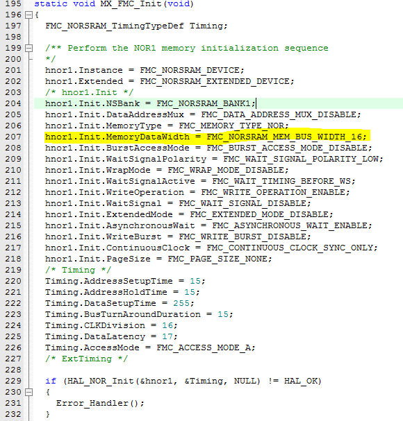
Yes, you can define the bus width of the FSMC bus, it won't increase the decoded region in memory, it simply shifts the address bits presented to the physical device.
For a memory larger than the 64MB decode window, you'll need to use TWO different decode regions and add glue logic to combine them at the device. ie drive the chip select as a combination of the two, and drive order address bit high or low depending on which one.
Up vote any posts that you find helpful, it shows what's working..
- Mark as New
- Bookmark
- Subscribe
- Mute
- Subscribe to RSS Feed
- Permalink
- Email to a Friend
- Report Inappropriate Content
2017-11-15 9:20 PM
- Mark as New
- Bookmark
- Subscribe
- Mute
- Subscribe to RSS Feed
- Permalink
- Email to a Friend
- Report Inappropriate Content
2017-11-16 8:58 AM
You'd need to AND a pair of -CS pins to drive the chip select on the memory, then a high order address bit could be one of the selects, being either 0 or 1 depending on the bank.
Each address in the ARM is a BYTE, when you configure the STM32 FSMC in 16-bit data mode it shifts the address bus as presented at the pins, thus A[0..25] at the pins are A[1..26] internally
Up vote any posts that you find helpful, it shows what's working..
- Mark as New
- Bookmark
- Subscribe
- Mute
- Subscribe to RSS Feed
- Permalink
- Email to a Friend
- Report Inappropriate Content
2017-11-16 10:18 PM
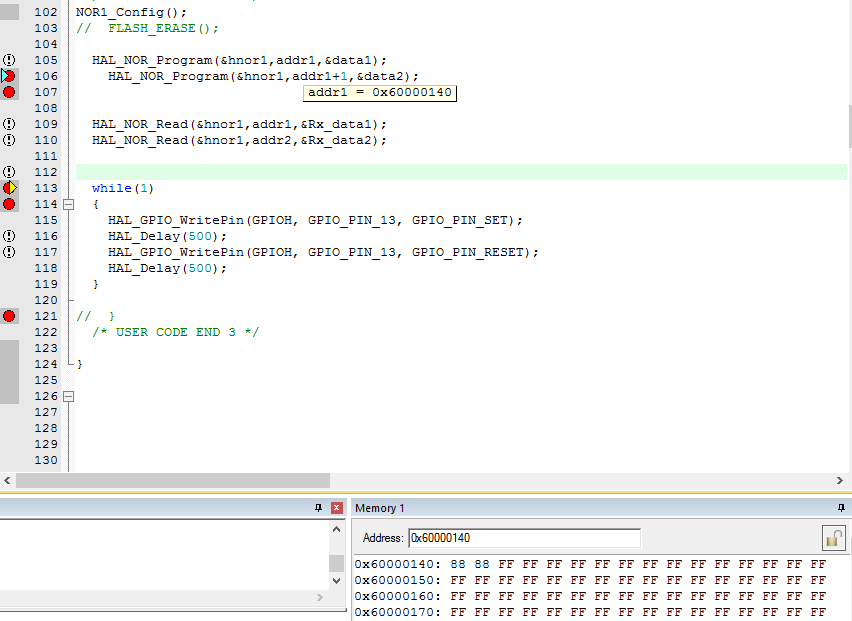
say i write 0xAAAA to location 0x0000000
, 0xCCCC to location 0x0000001
,0xFFFF(default) in location 0x0000002
it should be saved as AAAA , CCCC
but the data is stored as 0x8888 in location 0x0000000 which is the AND of 0xAAAA and 0xCCCC.
and if i read 0x0000001 location the data that i recieve is 0xFF88


So clearly, one write operation of a 16bit word is taking two address space.
and the contradicting issue is that, i cant go beyond 0x63FFFFFF also
because of this reason

i'm stuck with only 0x00 to 0x3FFFFFF addresses and i have to make use of only these numbers to address the entire 1Gbit Flash, ''
Each address in the ARM is a BYTE
'', yea so each incremental address is pointing to a byte. which is exactly 2^26 bytes, and tats only half of the memory!!!!- Mark as New
- Bookmark
- Subscribe
- Mute
- Subscribe to RSS Feed
- Permalink
- Email to a Friend
- Report Inappropriate Content
2017-11-17 6:05 AM
You'd have to write 16-bit words two bytes apart
[0x60000140] = 0xAAAA
[0x60000142] = 0xCCCC
Like I said, you'd need to combine two decode regions, this would require simple external logic.
Up vote any posts that you find helpful, it shows what's working..
- Getting started with STM32 - Basic questions in STM32 MCUs Products
- OCTOSPI as simple QUAD/Dual/Single parallel-to-serial output on STM32H5xx in STM32 MCUs Products
- 20 MSPS 8-bit External ADC on STM32H7R3V8T6 in STM32 MCUs Products
- PSSI Performance Benchmarks in STM32 MCUs Products
- STM32H7R3 PSSI RDY/DE bug in STM32 MCUs Products