- STMicroelectronics Community
- STM32 MCUs
- STM32 MCUs Products
- Guide for mapping a new chip as an external flash....
- Subscribe to RSS Feed
- Mark Topic as New
- Mark Topic as Read
- Float this Topic for Current User
- Bookmark
- Subscribe
- Mute
- Printer Friendly Page
Guide for mapping a new chip as an external flash. Is external loader required ?
- Mark as New
- Bookmark
- Subscribe
- Mute
- Subscribe to RSS Feed
- Permalink
- Email to a Friend
- Report Inappropriate Content
2024-03-04 6:34 AM
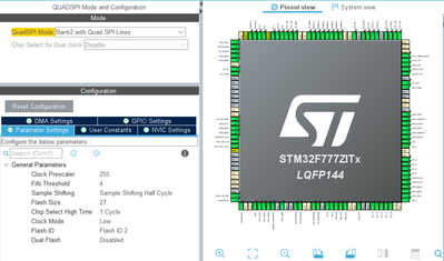
Hello I am in the task of adding a new flash as an external flash via QSPI interface with the MCU STM32F777ZITx.
The flash that I want to add is S25FL256L as an external flash. I am not finding any references which I can use with this flash. Also it is not getting clear to me whether I need to make an external loader for mapping the external flash in memory mapped mode or only configuration is needed ?
- Labels:
-
STM32F7 series
- Mark as New
- Bookmark
- Subscribe
- Mute
- Subscribe to RSS Feed
- Permalink
- Email to a Friend
- Report Inappropriate Content
2024-03-05 8:41 AM
But can you please provide a set of steps of getting it to work in memory mapped mode ?
I was able to extract the ID as 0x1 0x60 0x19.
And I also dont know what is the definition of
struct QSPI_FlashInfo
- Mark as New
- Bookmark
- Subscribe
- Mute
- Subscribe to RSS Feed
- Permalink
- Email to a Friend
- Report Inappropriate Content
2024-03-05 8:55 AM - edited 2024-03-05 9:15 AM
struct QSPI_FlashInfo {
  uint32_t EraseSectorSize;    /*!< Size of smallest sectors for the erase operation */
  uint32_t EraseSectorsNumber; /*!< Number of sectors for the erase operation */
  uint32_t ProgPageSize;       /*!< Size of page for the program operation */
  uint32_t ProgPagesNumber;    /*!< Number of pages for the program operation */
  uint32_t BigEraseSectorSize; /*!< Size of large sectors for the erase operation */
  uint32_t FlashSize;      /*!< Size of the flash in 4-byte addr mode, in bytes */
  uint8_t  DummyCycles;        /*!< Number of dummy cycles desired */
};

uint8_t BSP_QSPI_EnableMemoryMappedMode(void)
{
  QSPI_CommandTypeDef      s_command;
  QSPI_MemoryMappedTypeDef s_mem_mapped_cfg;

  /* Configure the command for the read instruction */
  s_command.InstructionMode   = QSPI_INSTRUCTION_1_LINE;
  s_command.Instruction       = QUAD_INOUT_FAST_READ_4_BYTE_ADDR_CMD;
  s_command.AddressMode       = QSPI_ADDRESS_4_LINES;
  s_command.AddressSize       = QSPI_ADDRESS_32_BITS;
  s_command.AlternateByteMode = QSPI_ALTERNATE_BYTES_NONE;
  s_command.AlternateBytesSize = QSPI_ALTERNATE_BYTES_8_BITS;
  s_command.AlternateBytes    = 0;
  s_command.DataMode          = QSPI_DATA_4_LINES;
  s_command.DummyCycles       = 8; //??? todo check
  s_command.DdrMode           = QSPI_DDR_MODE_DISABLE;
  s_command.DdrHoldHalfCycle  = QSPI_DDR_HHC_ANALOG_DELAY;
  s_command.SIOOMode          = QSPI_SIOO_INST_EVERY_CMD;

  /* Configure the memory mapped mode */
  s_mem_mapped_cfg.TimeOutActivation = QSPI_TIMEOUT_COUNTER_DISABLE;
  s_mem_mapped_cfg.TimeOutPeriod     = 0;

  if (HAL_QSPI_MemoryMapped(&QSPIHandle, &s_command, &s_mem_mapped_cfg) != HAL_OK)
  {
    return QSPI_ERROR;
  }
  /* Configure QSPI: LPTR register with the low-power time out value */
  WRITE_REG(QUADSPI->LPTR, 0xFFF);
  return QSPI_OK;
}
- Mark as New
- Bookmark
- Subscribe
- Mute
- Subscribe to RSS Feed
- Permalink
- Email to a Friend
- Report Inappropriate Content
2024-03-05 9:01 AM
Something like this
https://github.com/STMicroelectronics/stm32f769i-eval-bsp/blob/main/stm32f769i_eval_qspi.h#L98
Up vote any posts that you find helpful, it shows what's working..
- Mark as New
- Bookmark
- Subscribe
- Mute
- Subscribe to RSS Feed
- Permalink
- Email to a Friend
- Report Inappropriate Content
2024-03-05 7:56 PM
My experience (knowledge) when it comes to external flash memory:
- it CANNOT have any entry in linker script!
You cannot define a region with code on external flash: it CANNOT be loaded:
a) without to initialize the chip (some code has to be running first) - the external flash is not accessible
b) writing content to an external flash memory needs a special code (procedure) to "program" the flash - a debugger connected, e.g. via STM32CubeProgrammer, could flash some content:
a) this content comes from a different file (not you BIN file generated)
b) the tool will download code into MCU which will do at the end the programming - When you configure external Flash for "Memory Mapped": usually it is a Read-Only memory. In this mode you CANNOT write (flush) the external device.
- For writing (flushing) the external memory - you have to do in "indirect mode" (disable "memory mapped mode").
And it needs a special routine to do so (e.g. using command to erase pages, to write pages, to wait for done etc. It is not a RAM)
So, the usual way with (Read-Only) flash is this:
- flash the content to be stored on external flash:
a) via tools, e.g. STM32CubeProgrammer and selecting the right flash loader for this chip
b) do it yourself by getting code from PC (e.g. via UART, USB, ...) and flash it into external memory, with your
own flashing program - once this was done (once) - have a FW which enables external flash memory, e.g. a "memory mapped".
But never! place something in a linker script which would try to read from external flash memory (esp. not anything what would result in writing to external flash memory, e.g. global variable to initialize).
The flash memory becomes just available if your FW has booted and has initialized the flash memory. Any access before this is done will crash!
So, just when your FW with flash config has done all - you can execute any code line reading from external flash. Not during boot, not via linker script. It is like "adding external memory" after your MCU is up and running. Just when flash is configured - any access is possible.
- Mark as New
- Bookmark
- Subscribe
- Mute
- Subscribe to RSS Feed
- Permalink
- Email to a Friend
- Report Inappropriate Content
2024-03-06 12:45 AM
But this seems like a different chip for the external flash. I was asking if you had the same code that could help me setup the chip in memory mapped mode as per the code that you pasted above.
- Mark as New
- Bookmark
- Subscribe
- Mute
- Subscribe to RSS Feed
- Permalink
- Email to a Friend
- Report Inappropriate Content
2024-03-06 3:47 AM
But this seems like a different chip for the external flash. I was asking if you had the same code that could help me setup the chip in memory mapped mode as per the code that you pasted above. @Pavel A.
- Mark as New
- Bookmark
- Subscribe
- Mute
- Subscribe to RSS Feed
- Permalink
- Email to a Friend
- Report Inappropriate Content
2024-03-06 8:32 AM
I could see this but I think this is the single line reception mode.
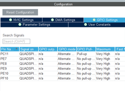
I still cant activate the QuadSPI
- Mark as New
- Bookmark
- Subscribe
- Mute
- Subscribe to RSS Feed
- Permalink
- Email to a Friend
- Report Inappropriate Content
2024-03-06 8:41 AM
There are literally dozens of examples of bringing up the QSPI interfaces, and initial command sequences to get the devices in the correct mode.
Typically enabling the 4-pin modes as devices start with 2-pins for data in/out. This is often NOT QUAD mode, but pin related. Most frequently done via bits in the Status Register(s)
Get the device into 4-byte address mode if bigger than 16MB
Then getting them into Quad mode to improved efficiency of command / address / data transfers, but often commands that are more flexible.
Finally for memory-mapped, creating a read templated for the most efficient Read transfer method.
Up vote any posts that you find helpful, it shows what's working..
- Mark as New
- Bookmark
- Subscribe
- Mute
- Subscribe to RSS Feed
- Permalink
- Email to a Friend
- Report Inappropriate Content
2024-03-06 8:55 AM - edited 2024-03-06 8:57 AM
You have to enable QUAD (pins) in Configuration Register 1, it's sticky, but you need to read it, make sure it's set and write it back.
Might want to double check the other status and configuration registers, if you use the wrong loader these can get set incorrectly, potentially write protecting blocks, or preventing erasure.
The 512Mb / 64MB device will need to get into 4-byte addressing mode, or you can use the 4-byte variants of the command to be explicit.
The part has a rich command set allowing for many possible permutations.
Up vote any posts that you find helpful, it shows what's working..
- Mark as New
- Bookmark
- Subscribe
- Mute
- Subscribe to RSS Feed
- Permalink
- Email to a Friend
- Report Inappropriate Content
2024-03-06 12:20 PM - edited 2024-03-06 1:11 PM
@rohan_m The posted code works with 32MB chip (SL25FL256L)
I don't have handy the 64 MB chip so cannot test. Please update the code (commands, values...) per the FL512 data sheet.
The device ID according to data sheet posted by Tesla is { 0x01, 0x02, 0x20, ??, 0, 0x80 }
If you read 0x1 0x60 0x19, then you have SL25FL256 (32 MB) rather than 512 (64 MB)?
The difference is important, these two have different erase block sizes and write block sizes!
Somebody (@Tesla DeLorean ?) IIRC wrote that the 512 Mb chip is a pair or 256 Mb glued together, this results in erase and write block size doubled *BUT* the poll operation is somehow badly affected, because you have to poll both chips instead of one?
*UPDATE* Sorry for confusion, you've mentioned that you have S25FL256L.
- STM32H757 SDMMC + FATFS consistently returns FR_NOT_READY in STM32 MCUs Embedded software
- Stm32h743iit6 preload at boot image background using LibJPeg in STM32 MCUs Embedded software
- PWM input output drift in STM32 MCUs Products
- STM32G431 Bootloader issue in STM32 MCUs Products
- TouchGFX Application Shows Black Screen After Bootloader Jump in STM32 MCUs TouchGFX and GUI


