- STMicroelectronics Community
- STM32 MCUs
- STM32 MCUs Products
- Guide for mapping a new chip as an external flash....
- Subscribe to RSS Feed
- Mark Topic as New
- Mark Topic as Read
- Float this Topic for Current User
- Bookmark
- Subscribe
- Mute
- Printer Friendly Page
Guide for mapping a new chip as an external flash. Is external loader required ?
- Mark as New
- Bookmark
- Subscribe
- Mute
- Subscribe to RSS Feed
- Permalink
- Email to a Friend
- Report Inappropriate Content
2024-03-04 6:34 AM
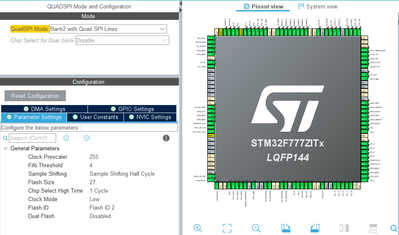
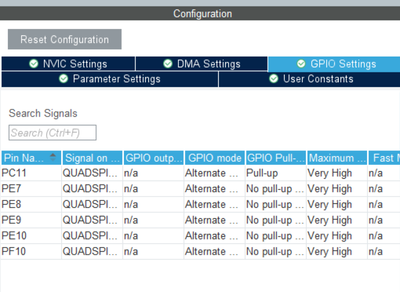
Hello I am in the task of adding a new flash as an external flash via QSPI interface with the MCU STM32F777ZITx.
The flash that I want to add is S25FL256L as an external flash. I am not finding any references which I can use with this flash. Also it is not getting clear to me whether I need to make an external loader for mapping the external flash in memory mapped mode or only configuration is needed ?
- Labels:
-
STM32F7 series
- Mark as New
- Bookmark
- Subscribe
- Mute
- Subscribe to RSS Feed
- Permalink
- Email to a Friend
- Report Inappropriate Content
2024-03-06 1:02 PM
Well there are some of those..
ST uses Micron MT25TLxxx parts that uses a pair of die side-by-side and 8-bit wide (dual mode), you have to read a status register from both chips, as a 16-bit compare mask/match operation, as data is interleaved at a byte level.
There are other Micron stacked-die parts in the 2Gbit and 4Gbit ranges now. Access in these chain one after the other, dividing the linear address space, you have to query these cyclically to ensure all die are idle.
Sorry, focused on the wrong part# not the one in the original post.
128Mb (16MB) would work with 3-byte addressing
256Mb (32MB) would need 4-byte addressing
Up vote any posts that you find helpful, it shows what's working..
- Mark as New
- Bookmark
- Subscribe
- Mute
- Subscribe to RSS Feed
- Permalink
- Email to a Friend
- Report Inappropriate Content
2024-03-06 1:35 PM - edited 2024-03-06 2:21 PM
Sorry for confusion. the OP has S25FL256L, not 512. So yes my code should work, after proper initialization of 4-pin mode and enable 32-bit address (this is optional, some prefer 2*16MB layout with 24-bit address). I have not posted the setup code, it is encumbered with unrelated stuff in my project.
** EDIT **
the problem with memory mapped mode can be in number of dummy cycles or alternate bits. Try to add alternate bits:
uint8_t BSP_QSPI_EnableMemoryMappedMode(void)
{
  QSPI_CommandTypeDef      s_command;
  QSPI_MemoryMappedTypeDef s_mem_mapped_cfg;

  s_command.InstructionMode   = QSPI_INSTRUCTION_1_LINE;
  s_command.Instruction       = QUAD_INOUT_FAST_READ_CMD;
  s_command.AddressMode       = QSPI_ADDRESS_4_LINES;
  s_command.AddressSize       = QSPI_ADDRESS_24_BITS;
  s_command.AlternateByteMode = QSPI_ALTERNATE_BYTES_4_LINES;  //<<< change
  s_command.AlternateBytesSize = QSPI_ALTERNATE_BYTES_8_BITS;
  s_command.AlternateBytes    = 0; //note see docum about the alt byte value
  s_command.DataMode          = QSPI_DATA_4_LINES;
  s_command.DummyCycles       = 8;
  s_command.DdrMode           = QSPI_DDR_MODE_DISABLE;
  s_command.DdrHoldHalfCycle  = QSPI_DDR_HHC_ANALOG_DELAY;
  s_command.SIOOMode          = QSPI_SIOO_INST_EVERY_CMD;

  /* Configure the memory mapped mode */
  s_mem_mapped_cfg.TimeOutActivation = QSPI_TIMEOUT_COUNTER_DISABLE;
  s_mem_mapped_cfg.TimeOutPeriod     = 0;

  if (HAL_QSPI_MemoryMapped(&QSPIHandle, &s_command, &s_mem_mapped_cfg) != HAL_OK)
  {
    return QSPI_ERROR;
  }
  /* Configure QSPI: LPTR register with the low-power time out value */
  WRITE_REG(QUADSPI->LPTR, 0xFFF);
  return QSPI_OK;
}
The sum of dummy cycles and alternate byte cycles defines where the output data bits begin. The same number will be with no alternate bytes but 10 dummy cycles instead of 8.
- Mark as New
- Bookmark
- Subscribe
- Mute
- Subscribe to RSS Feed
- Permalink
- Email to a Friend
- Report Inappropriate Content
2024-03-08 6:39 AM
Even with this function I am not able to enter the quad SPI transfer mode.
I still I am only using the single line mode. I think I will need to get rid of the quad mode register lock.
- « Previous
- Next »
- STM32H747 DSI 2-Lane Mode Issues with CO5300 Display Driver in STM32 MCUs Embedded software
- USB OTG HS Host: PENA cleared spuriously at HFNUM=16383 with ULPI PHY (USB3300) in STM32 MCUs Embedded software
- STM32H757 SDMMC + FATFS consistently returns FR_NOT_READY in STM32 MCUs Embedded software
- Stm32h743iit6 preload at boot image background using LibJPeg in STM32 MCUs Embedded software
- PWM input output drift in STM32 MCUs Products


