- STMicroelectronics Community
- STM32 MCUs
- STM32 MCUs Products
- Re: GPIO state at power down
- Subscribe to RSS Feed
- Mark Topic as New
- Mark Topic as Read
- Float this Topic for Current User
- Bookmark
- Subscribe
- Mute
- Printer Friendly Page
GPIO state at power down
- Mark as New
- Bookmark
- Subscribe
- Mute
- Subscribe to RSS Feed
- Permalink
- Email to a Friend
- Report Inappropriate Content
2018-02-03 2:40 PM
Hello there,
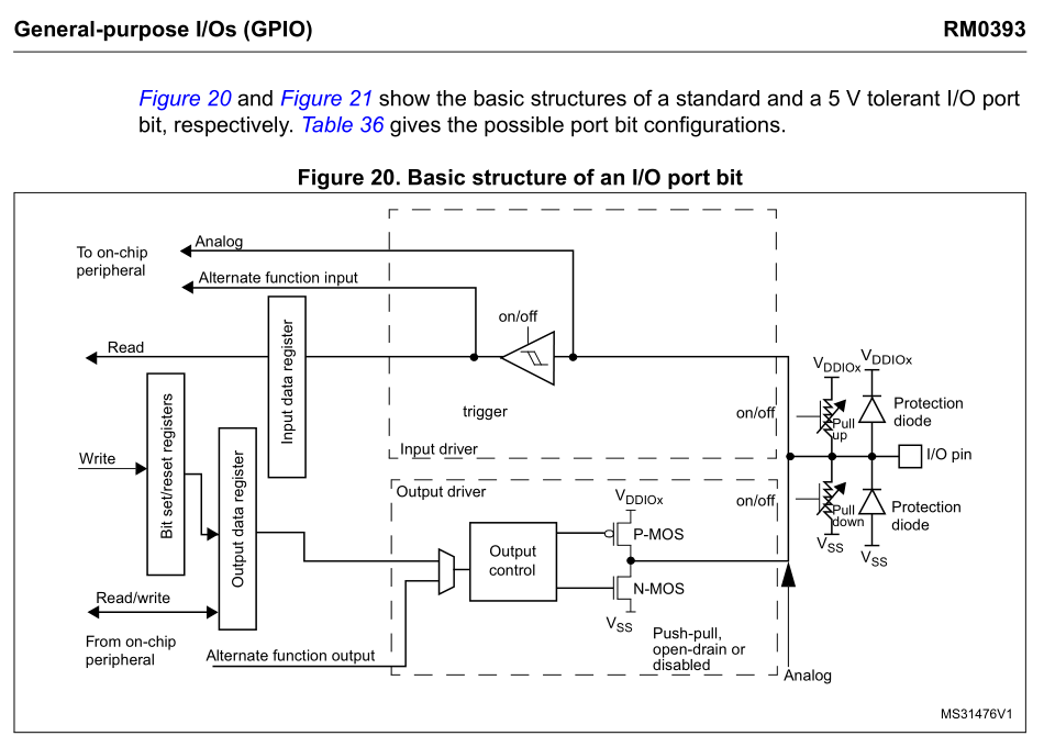
According to the datasheet, the GPIO ports circuit diagram looks like this in STM323L4x2:

From this diagram I understand that at powerdown (VCC = VSS = 0 V) the I/O pin state is high impedance. But is that 100% correct? I want to make sure before I make a design move that would save me some components. But for this I need to know either there are no internal pull-downs on a pin when the MCU is powered down.
I would appreciate all help.
#gpio #io #stm32l4- Labels:
-
GPIO-EXTI
-
STM32L4 Series
- Mark as New
- Bookmark
- Subscribe
- Mute
- Subscribe to RSS Feed
- Permalink
- Email to a Friend
- Report Inappropriate Content
2018-02-03 10:39 PM
My 2 cents: When the supply voltage is equal to its ground, you typically get in most electronic programmable components the ESD protection back to back diods or equivalent. If you want to confirm this, take any board, short VDD to GND and run a diod check with a multimeter.
For I2C dedicated pins or oscillator pins, the protection may be different behaviour which you can too check easily through spec and confirm with diod check (which is also sometime used to test soldering pin is ok).
- Mark as New
- Bookmark
- Subscribe
- Mute
- Subscribe to RSS Feed
- Permalink
- Email to a Friend
- Report Inappropriate Content
2018-02-04 12:12 AM
Hi Lukasz,
State of GPIOs for STM32L4 MCUs:
- under reset- high impedance
- just after start up (when the Power On Reset is released) - analog input
- in application - according to user configuration
Exceptions could be special functions pins: NRST pin , BOOT0 pin , Debug (JTAG, SWD) pins, oscillator pins. For example at least one of JTAG lines (PA15, which acts as JTDI) has a pull-up in reset state in order to activate debug session under reset.
Regards
Szymon- Mark as New
- Bookmark
- Subscribe
- Mute
- Subscribe to RSS Feed
- Permalink
- Email to a Friend
- Report Inappropriate Content
2018-02-04 2:02 AM
Hello Szymon,
Thank you for answer. I understand reset state is equal to powered down state.
- Mark as New
- Bookmark
- Subscribe
- Mute
- Subscribe to RSS Feed
- Permalink
- Email to a Friend
- Report Inappropriate Content
2018-02-04 2:21 AM
You're welcome. Yes, I confirm:
reset state = power down state.
Regards
Szymon
- Mark as New
- Bookmark
- Subscribe
- Mute
- Subscribe to RSS Feed
- Permalink
- Email to a Friend
- Report Inappropriate Content
2018-02-05 7:39 AM
Szymon,
reset state = power down state
Lukasz asked for powered down state (VCC = VSS = 0 V).
In that case, KIC's answer from above applies.
JW
- Mark as New
- Bookmark
- Subscribe
- Mute
- Subscribe to RSS Feed
- Permalink
- Email to a Friend
- Report Inappropriate Content
2018-02-05 10:12 AM
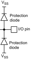
Do you guys mean this?

- Mark as New
- Bookmark
- Subscribe
- Mute
- Subscribe to RSS Feed
- Permalink
- Email to a Friend
- Report Inappropriate Content
2018-02-05 10:42 AM
Yes.
The 5V-tolerant pins don't have the upper diode connected directly to VDD(IO) - there is some undisclosed protection circuitry though. Note the requirement for maximum Input voltage on FT_xxx pins in DS - it's something like 'the lowest of supply voltages plus some particular value (e.g. 4.0V for 'L476)'. That hints that the protection may be equivalent to a 4.0V Zener diode (in series with a reverse-polarized ideal diode).
Also note, that unless you provide external hard short (which would be very unusual), there's no guarantee for VDD=VSS just because you don't supply current explicitly through the VDD pins. Once you start to push current through the protection circuitry/diodes to VDD, that voltage may quite well rise up to the point where the mcu starts to work. As usually there's not enough current to support full-scale run of the mcu, depending on particular circumstances it may start some oscillations of sort.
JW
- Mark as New
- Bookmark
- Subscribe
- Mute
- Subscribe to RSS Feed
- Permalink
- Email to a Friend
- Report Inappropriate Content
2018-02-05 10:48 AM
Thank you for answer,
Yes in fact I am not ground the VCC pin. I am only closing the P Fet providing positive voltage value. By saying that VCC = VSS, i meant with pulldowns.
- Validating wiring for temperate control unit in STM32 MCUs Motor control
- STM32F767 LwIP TCP Client in STM32 MCUs Embedded software
- HAL_SPI_Transmit() returns HAL_ERROR STM32H7R3V8H6 in STM32 MCUs Products
- STM32WB55 FUS Corrupted After Register Modifications – Unable to Upgrade in STM32 MCUs Boards and hardware tools
- STM32U575 USB battery charge detect fails on the second connection. in STM32 MCUs Embedded software