- STMicroelectronics Community
- STM32 MCUs
- STM32 MCUs Products
- Re: ALTERNATE FUNCTION CONFUSION
- Subscribe to RSS Feed
- Mark Topic as New
- Mark Topic as Read
- Float this Topic for Current User
- Bookmark
- Subscribe
- Mute
- Printer Friendly Page
ALTERNATE FUNCTION CONFUSION
- Mark as New
- Bookmark
- Subscribe
- Mute
- Subscribe to RSS Feed
- Permalink
- Email to a Friend
- Report Inappropriate Content
2010-10-13 12:56 AM
ALTERNATE FUNCTION CONFUSION
- Mark as New
- Bookmark
- Subscribe
- Mute
- Subscribe to RSS Feed
- Permalink
- Email to a Friend
- Report Inappropriate Content
2011-05-17 05:11 AM
1.- how does the micro
distinguish I2C1_SCL and USART_TX
1.
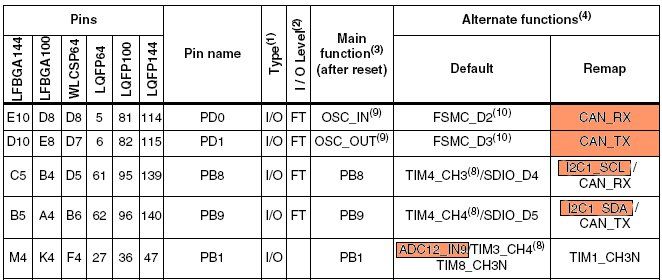
The peripherial that is enabled takes control over the pins. Simply do not enable another peripherial on the same pins.2.- And if my I2C_SCL and I2C_SDA pins are PB8 and PB9, how must I configure it??You will have to remap the I2C1 pins to PB8/9: GPIO_PinRemapConfig(GPIO_Remap_I2C1, ENABLE);
- Mark as New
- Bookmark
- Subscribe
- Mute
- Subscribe to RSS Feed
- Permalink
- Email to a Friend
- Report Inappropriate Content
2011-05-17 05:11 AM
this remapping confuses me much too
compare with TMS320F2000 from Texas Instruments only one alternate function is enabled at the port pin at the same time even if 2 peripherals are enabled at the same time or not- Mark as New
- Bookmark
- Subscribe
- Mute
- Subscribe to RSS Feed
- Permalink
- Email to a Friend
- Report Inappropriate Content
2011-05-17 05:11 AM
ONLY PINS CONFIGURATION
GPIO_InitStructure.GPIO_Speed = GPIO_Speed_50MHz;
/*--------------------------------------------------------------------------------- PD.0 / PD.1-------- */ GPIO_PinRemapConfig(GPIO_Remap1_CAN,ENABLE); // THAT OR THE FOLLOWING? GPIO_PinRemapConfig(GPIO_Remap2_CAN,ENABLE); /* --- Configure CAN pin: RX ---------------- */GPIO_InitStructure.GPIO_Pin = GPIO_Pin_0; GPIO_InitStructure.GPIO_Mode = GPIO_Mode_IPU; GPIO_Init(GPIOD, &GPIO_InitStructure); /* --- Configure CAN pin: TX ---------------- */ GPIO_InitStructure.GPIO_Pin = GPIO_Pin_1; GPIO_InitStructure.GPIO_Mode = GPIO_Mode_AF_PP; GPIO_Init(GPIOD, &GPIO_InitStructure);
/*--------------------------------------------------------------------------------- PB.0 / PB.09 -------- */ GPIO_PinRemapConfig(GPIO_Remap_I2C1,ENABLE); GPIO_InitStructure.GPIO_Pin = GPIO_Pin_8 | GPIO_Pin_9; GPIO_InitStructure.GPIO_Speed = GPIO_Speed_50MHz; GPIO_InitStructure.GPIO_Mode = GPIO_Mode_AF_OD; GPIO_Init(GPIOB, &GPIO_InitStructure); /*----------------------------------------------------------------------------------------------- PB.01 ----- */ GPIO_InitStructure.GPIO_Pin = GPIO_Pin_1; /* PB.01 ADC CHANNEL 9 */ GPIO_InitStructure.GPIO_Mode = GPIO_Mode_AIN; /* ANALOG INPUT */ GPIO_Init(GPIOC, &GPIO_InitStructure); /*--------------------------------------------------------------------------------------------------------------- */ FOLLOW THE NEXT FIGURE

- Mark as New
- Bookmark
- Subscribe
- Mute
- Subscribe to RSS Feed
- Permalink
- Email to a Friend
- Report Inappropriate Content
2011-05-17 05:11 AM
If you want to use a port pin for alternate function, you
always
have to configure it: * For peripherial outputs (like Usart TX, SPI CLK) normally AF_PP or AF_OD must be used. This disconnects the pin driver from the GPIO and connects it to the peripherial * For inputs (e.g. RX, SPI MISO) normally IN_FLOATING, sometimes IPU/IPD is required. (BTW: This means that reading the state of the GPIO pin is still possible) Chapter 8.1.11 in the Useguide shows the configuration for every peripherial. (you will find I2C listed with AF_OD there) With remapping, you simply route the peripherial lines to another port. Sometimes you have more than one choice. CAN is initially found on PA11/12 and might go to PB8/9 or PD0/1 when remapped. This is the reason why GPIO_Remap1_CAN (for PB8/9) and GPIO_Remap2_CAN (for PD0/1) exist. And to make things even more complicated, some peripherials can be partially remapped...- Mark as New
- Bookmark
- Subscribe
- Mute
- Subscribe to RSS Feed
- Permalink
- Email to a Friend
- Report Inappropriate Content
2011-05-17 05:11 AM
Hi and thaks for the quick reply. I´m so glad for oyur help. Can you tell me what document is Userguide?
I´ve Hitex insider´s guide, RM0008 and the datasheet. Can you give me the link to this document?- Mark as New
- Bookmark
- Subscribe
- Mute
- Subscribe to RSS Feed
- Permalink
- Email to a Friend
- Report Inappropriate Content
2011-05-17 05:11 AM
Ups, the word ''Userguide'' is wrong here... worked a little bit too much with TI controllers in the past. It should be ''Reference Manual'' (RM0008
)- Not Receiving UART message from STM32WL5M to Laptop in STM32 MCUs Wireless
- I2C between two NUCLEO-F446RE boards in STM32 MCUs Boards and hardware tools
- Enable ITM printf output using openocd/gdb on STM32H7 in STM32CubeIDE (MCUs)
- Changing I/O pin function in Riverdi example causes build error in STM32 MCUs TouchGFX and GUI
- CAN START Probem in STM32 MCUs Products