- STMicroelectronics Community
- STM32 MCUs
- STM32 MCUs Embedded software
- Re: Help on a schematic for dev-board based on STM...
- Subscribe to RSS Feed
- Mark Topic as New
- Mark Topic as Read
- Float this Topic for Current User
- Bookmark
- Subscribe
- Mute
- Printer Friendly Page
Help on a schematic for dev-board based on STM32G431 with USB-C power delivery and programming features
- Mark as New
- Bookmark
- Subscribe
- Mute
- Subscribe to RSS Feed
- Permalink
- Email to a Friend
- Report Inappropriate Content
2020-05-24 10:27 AM
Hello,
I am making a dev board for this new family of MCU, I need USB programming and power delivery.
To make it I am referring to the datasheet, Nucleo dev board and to the application note.
I did only once a board with STM32 and it was an F1. I can see that there are many differences, so I thought to open a topic to gather some more suggestions.
This is what I have so far: high quality pic of the schematics
1) Pull up for DP
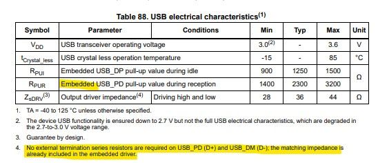
Back in the F1 boards I had to put a pull-up 1.5k resistor between DP and 3.3V, now it seems that the needed circuit is already provided inside the package. Si I can remove R1, R2 and R5. Is it correct or did I misunderstood it? What about the 2 cap (C13, C14)?
2) CC1 and CC2 pins for power delivery
Should I wire the CCx to UCPD1_DBCCx or to UCPD1_CCx? Which is the difference?
3) VREF pin usage
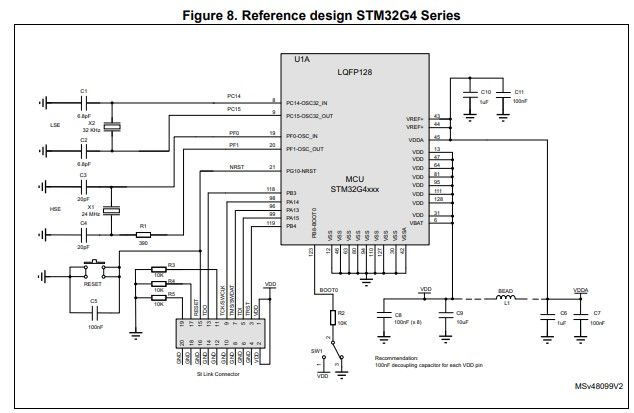
I can have this pin connected to VDDA or to an external source (plus 2 cap):
"If JP2 is closed then C10 and C11 doesn't have to be populated"
4) BOOT0 pin wiring
I think I should wire this pin to GND for normal operation and to 3.3V for uploading of new code. I think I would do it with a header-jumper but other suggestion (or correction) are welcomed
5) GND and AGND connection
I think that I would get different answer on this. I saw a lot of people making a single GND/AGND and also someone make a single point connection between them
I would like to share the schematics/board if you think it would be useful
- Labels:
-
Documentation
-
STM32G4 series
-
USB-PD
- Mark as New
- Bookmark
- Subscribe
- Mute
- Subscribe to RSS Feed
- Permalink
- Email to a Friend
- Report Inappropriate Content
2020-05-24 12:23 PM
> 1) Pull up for DP
You can remove everything on that line. If you want additional ESD protection, put a dedicated chip on the data lines for that. Take a look at AN4879.
> 3) VREF pin usage
Typically this is directly connected to VDDA. Same notes as in (5) below.
> 4) BOOT0 pin wiring
If you're programming over SWD, you can hook this straight to GND. Only reason you need to pull it up is to enable the system bootloader.
> 5) GND and AGND connection
If you're not using the ADC/DAC or if you don't need more than about 10 bits of precision, it doesn't really matter how you ground AGND. I put a via to the ground plane right at the pin.
- Mark as New
- Bookmark
- Subscribe
- Mute
- Subscribe to RSS Feed
- Permalink
- Email to a Friend
- Report Inappropriate Content
2020-05-27 11:26 AM
I just updated the question with a pic of the last schematics, as @TDK suggested.
> 1) Pull up for DP
I removed all the resistors on the DM/DP lines but I keept the two capacitors, should I remove also them?
> 3) VREF pin usage
I would do as you suggest and I will keep the JP2 closed, also this is the same as the reference design from STM
> 4) BOOT0 pin wiring
I would mainly use the bootloader so I would need to switch in a simple way the BOOT0 pin
> 5) GND and AGND connection
10 bits would be more than enough, I will be using the common GND
If you still have any suggestions please I will follow
EDIT: found the solution for the CCx pins here. I think I will implement the TCPP01 in my design
- Custom STSPIN32 Board flashing not working in STM32 MCUs Motor control
- STM32U575 chip short when JTAG Connected in STM32 MCUs Boards and hardware tools
- STM32F411 firmware download issue in DFU mode in STM32 MCUs Products
- STM32H7 base schematic review in STM32 MCUs Boards and hardware tools
- [STM32G431] Programming issue in STM32 MCUs Products

