- STMicroelectronics Community
- STM32 MCUs
- STM32 MCUs Boards and hardware tools
- STM32L4 Series: Using DMA to copy from Flash to SR...
- Subscribe to RSS Feed
- Mark Topic as New
- Mark Topic as Read
- Float this Topic for Current User
- Bookmark
- Subscribe
- Mute
- Printer Friendly Page
STM32L4 Series: Using DMA to copy from Flash to SRAM
- Mark as New
- Bookmark
- Subscribe
- Mute
- Subscribe to RSS Feed
- Permalink
- Email to a Friend
- Report Inappropriate Content
2023-09-26 11:50 AM
Hi there,
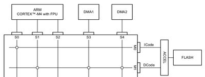
Looking into the TRM for the STM32L412xx board, I was wondering if I could use a DMA to copy constant data from the Flash to SRAM. The system architecture block diagram connects the DMAs to Flash through the DCode path:
However, while reading the document it is explicit mentioned this for the DMA bus:
This bus connects the AHB master interface of the DMA to the BusMatrix.The targets of this bus are the SRAM1 and SRAM2, the AHB1 peripherals including the APB1 and APB2 peripherals, the AHB2 peripherals and the external memories through the QUADSPI.
This got me confused. Can someone explain these details? Is it possible or not to read from Flash using the DMAs, and if not, why is the DMA seems to be connected to the embedded Flash through the DCode path?
Solved! Go to Solution.
- Labels:
-
STM32L4 series
Accepted Solutions
- Mark as New
- Bookmark
- Subscribe
- Mute
- Subscribe to RSS Feed
- Permalink
- Email to a Friend
- Report Inappropriate Content
2023-09-26 12:02 PM - edited 2023-09-26 12:06 PM
Yes, you can use the DMA to transfer from FLASH to SRAM.
- Mark as New
- Bookmark
- Subscribe
- Mute
- Subscribe to RSS Feed
- Permalink
- Email to a Friend
- Report Inappropriate Content
2023-09-26 12:02 PM - edited 2023-09-26 12:06 PM
Yes, you can use the DMA to transfer from FLASH to SRAM.
- Mark as New
- Bookmark
- Subscribe
- Mute
- Subscribe to RSS Feed
- Permalink
- Email to a Friend
- Report Inappropriate Content
2023-09-26 12:04 PM - edited 2023-09-26 12:23 PM
- Mark as New
- Bookmark
- Subscribe
- Mute
- Subscribe to RSS Feed
- Permalink
- Email to a Friend
- Report Inappropriate Content
2023-09-27 2:41 AM
Thanks for the clarification!
- Mark as New
- Bookmark
- Subscribe
- Mute
- Subscribe to RSS Feed
- Permalink
- Email to a Friend
- Report Inappropriate Content
2023-11-03 10:31 AM - edited 2023-11-03 10:34 AM
Hi TDK,
I was doing some random experiments and during a series of stress tests I encountered some results that I can't fully understand.
The experimental setup is simple: the CPU is running a sequence of 100 nop instructions while I would enable/disable the number of active DMAs and mix-and-match acceleration options of the Flash controller (instruction cache, data cache, and prefetching). DMAs are configured to be reading data from flash and writing it to the SRAM. When the transfer is over, the DMA's interrupt is triggered, and I reconfigure them all over again and start the transfer again. I use the systick to measure the time taken to execute that 100 nop instructions
When doing that, I achieve some results that I can't explain:
- With a single active DMA, there was a 30% overhead in performance, which seems reasonable since the core is sharing with the DMA the access to the flash
- Activating a second DMA caused the execution delay to spike nearly to 1000x, which I wasn't expecting and couldn't quite figure out why is this happening
- Disabling the instruction and data cache resulted in total core starvation, meaning I couldn't get any output from the serial port with the total number of cycles that took to run the 100 nop instructions.
Notably, when only the data cache was enabled, the system's performance improved compared to having only the instruction cache active.
Given these observations, I am curious to understand the underlying reasons for this behavior. So, I'm shooting these questions:
- Why does the system performance degrade so significantly when a second DMA is activated?
- What could be the cause behind the complete core starvation when the ART acceleration options are disabled?
- Is there a reason why the data cache seems to have a more substantial impact on performance than the instruction cache in this context?
Any technical insights, guidance, or suggestions for further experimentation would be greatly appreciated. Thank you for your time and sorry for the long explanation.
- STM32H755 USB CDC Help in STM32 MCUs Embedded software
- Boot Mode Error in Cube Programmer. in STM32 MCUs Boards and hardware tools
- STM32L476RCT6 – HAL_Delay and UART Blocking Issue on Custom Board in STM32 MCUs Embedded software
- Booting from the Main Flash Memory on the STM32L4 in STM32 MCUs Products
- NUCLEO-L452RE-P current consumption way more than expected - ~ 20µA - 30µA in Shutdown Mode in STM32 MCUs Products
