- STMicroelectronics Community
- Product forums
- ST25 NFC/RFID tags and readers
- Re: st25r3911B hardware deseign example
- Subscribe to RSS Feed
- Mark Topic as New
- Mark Topic as Read
- Float this Topic for Current User
- Bookmark
- Subscribe
- Mute
- Printer Friendly Page
st25r3911B hardware deseign example
- Mark as New
- Bookmark
- Subscribe
- Mute
- Subscribe to RSS Feed
- Permalink
- Email to a Friend
- Report Inappropriate Content
2020-09-25 03:29 AM
Hello!
I'm trying to develop my own PCB. Now I'm drawing an electrical scheme.
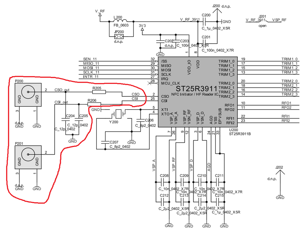
Now, I'm watching "X-CUBE NFC05A1" electrical scheme (LINK).
I have two questions:
1) Is there any other document how to draw electrical scheme for st25r3911B chip?
2) If I don't want to use "capacitive Wake-Up", do I need just to "skip" the red-crossed part on the picture below and leave pins CSO,CSI open or I need to use some other components?
All the best,
Domen
Solved! Go to Solution.
Accepted Solutions
- Mark as New
- Bookmark
- Subscribe
- Mute
- Subscribe to RSS Feed
- Permalink
- Email to a Friend
- Report Inappropriate Content
2020-09-29 12:14 AM
Hello Domen,
Looks good.
You might can replace L1 by a 0R resistor. If you have too much filtering ( too much DC resistance in the supply) you might end up with ~4V at pin 8 (3911B VDD pin).
But this can be adjusted in the BOM.
When doing the layout you should take care that C28 and C32 are very close to the IC. I would recommend a similar layout as on the ST25R3911B-DISCO board.
Those caps are the driver decoupling capacitors and will have the most influence on switching noise due to the transmiter. They should have a solid connection to VSP_RF and VSN_RF.
Also C13 and C14 should be kept very close and on the same plane as the IC.
BR Travis
- Mark as New
- Bookmark
- Subscribe
- Mute
- Subscribe to RSS Feed
- Permalink
- Email to a Friend
- Report Inappropriate Content
2020-09-28 01:13 AM
Hello Domen,
If the capacitive sensing is not needed, all components can be left d.n.p. or even removed.
You can also use the electrical scheme of the ST25R3911B-DISCO but it shows a very similar schematic.
The UFL connector (P200, P201) have two purpose:
1.) Connect external capacitive patches
2.) Connect an oscilloscope to observe internal test (receiver) signals.
As you said, #1 is not required for your application.
For #2 I would recommend to place test points with very short traces close to the CSI and CSO pin.
If necessary you can connect wires or directly probe with a high impedance probe.
I would not recommend to add some long traces to the CSI / CSO pins.
br Travis
- Mark as New
- Bookmark
- Subscribe
- Mute
- Subscribe to RSS Feed
- Permalink
- Email to a Friend
- Report Inappropriate Content
2020-09-28 10:36 PM
Thank you for your informations Travis. It's very useful!.
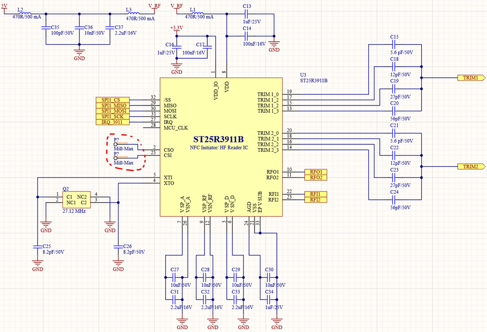
I did it like It is in the picture below. Hope It's okey :)
Best regards,
DomenI
- Mark as New
- Bookmark
- Subscribe
- Mute
- Subscribe to RSS Feed
- Permalink
- Email to a Friend
- Report Inappropriate Content
2020-09-29 12:14 AM
Hello Domen,
Looks good.
You might can replace L1 by a 0R resistor. If you have too much filtering ( too much DC resistance in the supply) you might end up with ~4V at pin 8 (3911B VDD pin).
But this can be adjusted in the BOM.
When doing the layout you should take care that C28 and C32 are very close to the IC. I would recommend a similar layout as on the ST25R3911B-DISCO board.
Those caps are the driver decoupling capacitors and will have the most influence on switching noise due to the transmiter. They should have a solid connection to VSP_RF and VSN_RF.
Also C13 and C14 should be kept very close and on the same plane as the IC.
BR Travis
- Mark as New
- Bookmark
- Subscribe
- Mute
- Subscribe to RSS Feed
- Permalink
- Email to a Friend
- Report Inappropriate Content
2020-09-29 03:22 AM
Thank you. You send the message just before I want to submit board to be made :)
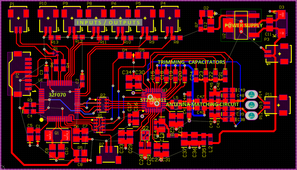
I removed the L1, and move the condensators (C28, C32, C13, C14) even closer to the chip.
The picture below represent the PCB :)
Best regarts,
DomenI
- Practical implementation of NAND using FMC in STM32H723 in STM32 MCUs Products
- Failing to implement HAL_PKA_ECCCompleteAddition correctly in STM32 MCUs Security
- LIS3DH FIFO Full Interrupt in MEMS (sensors)
- STM32F103C8T6 Blue Pill Not Detected After Flashing MAX31855 SPI Sample Code in Others: hardware and software
- Replacement for STM32F105 in STM32 MCUs Products


