- STMicroelectronics Community
- Product forums
- Power management
- Re: Shoot Through - Bootstrap Capacitance Question
- Subscribe to RSS Feed
- Mark Topic as New
- Mark Topic as Read
- Float this Topic for Current User
- Bookmark
- Subscribe
- Mute
- Printer Friendly Page
Shoot Through - Bootstrap Capacitance Question
- Mark as New
- Bookmark
- Subscribe
- Mute
- Subscribe to RSS Feed
- Permalink
- Email to a Friend
- Report Inappropriate Content
2021-03-31 06:39 AM
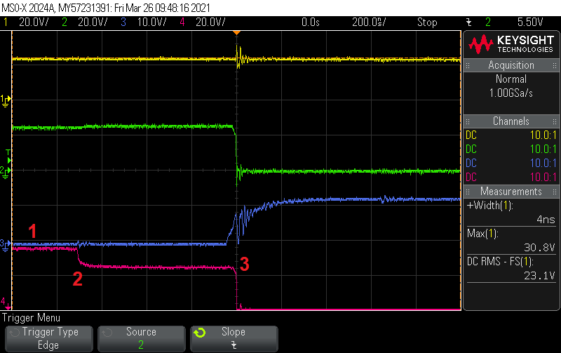
I'm seeing shoot through on the coil drives for the STSPIN32F0A custom implementation in the attached schematic. The attached scope shot has these channels:
CH1: 24V
CH2: Coil
CH3: Low Side Gate
CH4: High Side Gate
You can see the 700ns of deadtime when the high side gate drive drops from 35V to 24V. If the gate was just held up capacitively, the diode should be conducting there bringing it to near zero, but instead it is perfectly flat, not held up capacitively but appears driven. I wonder if this if this relates to the bootstrap capacitor somehow buggering the high side gate drive. I’m not familiar with these bootstrap circuits. How does one determine the correct bootstrap capacitance? Also, I noticed the STEVAL-3201 high side gate isn't boosted to 35V but instead is 24V or 0V.
Solved! Go to Solution.
- Labels:
-
Motor Control Hardware
Accepted Solutions
- Mark as New
- Bookmark
- Subscribe
- Mute
- Subscribe to RSS Feed
- Permalink
- Email to a Friend
- Report Inappropriate Content
2021-04-06 02:20 AM
Hi @WSega.1 and welcome to the ST Community !
Seems to me that everything is working fine.
You are measuring the HS gate driver referred to GND so it is expected that double step 36V down to 24V.
The HS driver works respect to OUT_x pin (the coil of the motor), that is the source of the HS MOSFET.
Indeed, the gate driver drives the Vgs of the MOSFET, that is the reason why the HS driver is refereed to OUT (coil) instead of GND.
Here is your screenshot adding 3 reference points described here below:

- HS driver on, LS driver off, and OUT pin (Coil) at the supply voltage 24V. The voltage of the gate drivers, hence the target Vgs of the MOSFETs, is 12V. So, you have the HS driver at 24V + 12V about 36V on CH4.
- Turn off the HS driver but the OUT pin is still high at 24V (probably current is flowing in the HS, turning on the bulk diode of the HS). In this case the HS gate driver stays goes to 24V (0V respect to OUT).
- After the deadtime, the LS driver turns on (up to 12V), the OUT falls to 0V and consequently the HS driver falls to 0V in the same way.
Basically the bootstrap capacitor is referred to the OUT node, and when it switches high to the supply (24V in the example) it can provide a voltage higher than the supply itself.
When the HS driver is on, the bootstrap capacitor slowly discharges: this is the reason why it is not possible to keep on continuously the HS MOSFET.
Of course this is a limitation, but not so critical in many switching systems.
The size of the bootstrap capacitor basically depends on the maximum time your application needs to keep on the HS driver, the total gate charge of the MOSFET driven and the maximum drop allowed on the bootstrap voltage.
I hope this explanation can solve your doubts; if so, consider to mark this post as "best answer" by clicking the label here below.
- Mark as New
- Bookmark
- Subscribe
- Mute
- Subscribe to RSS Feed
- Permalink
- Email to a Friend
- Report Inappropriate Content
2021-04-06 02:20 AM
Hi @WSega.1 and welcome to the ST Community !
Seems to me that everything is working fine.
You are measuring the HS gate driver referred to GND so it is expected that double step 36V down to 24V.
The HS driver works respect to OUT_x pin (the coil of the motor), that is the source of the HS MOSFET.
Indeed, the gate driver drives the Vgs of the MOSFET, that is the reason why the HS driver is refereed to OUT (coil) instead of GND.
Here is your screenshot adding 3 reference points described here below:

- HS driver on, LS driver off, and OUT pin (Coil) at the supply voltage 24V. The voltage of the gate drivers, hence the target Vgs of the MOSFETs, is 12V. So, you have the HS driver at 24V + 12V about 36V on CH4.
- Turn off the HS driver but the OUT pin is still high at 24V (probably current is flowing in the HS, turning on the bulk diode of the HS). In this case the HS gate driver stays goes to 24V (0V respect to OUT).
- After the deadtime, the LS driver turns on (up to 12V), the OUT falls to 0V and consequently the HS driver falls to 0V in the same way.
Basically the bootstrap capacitor is referred to the OUT node, and when it switches high to the supply (24V in the example) it can provide a voltage higher than the supply itself.
When the HS driver is on, the bootstrap capacitor slowly discharges: this is the reason why it is not possible to keep on continuously the HS MOSFET.
Of course this is a limitation, but not so critical in many switching systems.
The size of the bootstrap capacitor basically depends on the maximum time your application needs to keep on the HS driver, the total gate charge of the MOSFET driven and the maximum drop allowed on the bootstrap voltage.
I hope this explanation can solve your doubts; if so, consider to mark this post as "best answer" by clicking the label here below.
- Mark as New
- Bookmark
- Subscribe
- Mute
- Subscribe to RSS Feed
- Permalink
- Email to a Friend
- Report Inappropriate Content
2021-04-11 06:44 AM
Thanks for the great response, Dario. I follow your logic about the HS drive dropping to 24V which turns off the high side FET, but I wonder what is causing the perturbance on the 24V (CH1) which looks like it is caused by a loading event such as shoot through. The perturbance is only there when there is a 'shoulder' or flat 24V on the HS between points 2 and 3 on your marked up screenshot. You mentioned the bulk diode of the HS FET conducting during this time, can you give some more detail on that and how we might mitigate it? Do you mean conducting source to drain on the FET?
- Mark as New
- Bookmark
- Subscribe
- Mute
- Subscribe to RSS Feed
- Permalink
- Email to a Friend
- Report Inappropriate Content
2021-04-16 04:47 AM
Hi @WSega.1
Currents flowing in the FET's bulk diodes is a normal consequence when working with inductive loads.
Since the inductor stores magnetic energy, it is not possible to change the current flowing in it immediately.
As a result, when both power FETs are turned off (during deadtime) the current must flow somewhere and it goes in one of the two bulk diode.
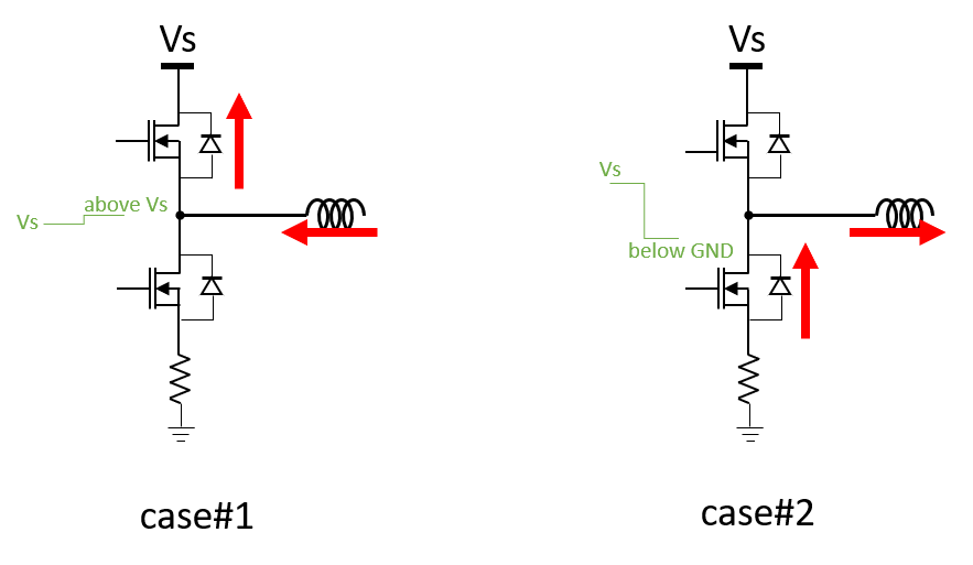
Referring to your screenshot (high to low transition of the coil), you can have two different possibilities:
- Case #1 (yours): the current is flowing in the power stage.
- Case #2: the current is flowing out of the power stage.

As you can see in Case#2, the voltage on the coil (CH2) is driven low by the bulk diode of the low side FET, immediately at the beginning of the dead time, as soon as the high side FET is turned off.
This means that you will not see the long 700ns “shoulder “ on the HS driver.
In Case#1, during the deadtime the voltage on the coil (CH2) stay slightly higher than Vs because of the bulk diode.
If you look carefully you can see it on CH2 between point 2 and point 3 in the previous image.
In this case, what brings low the coil voltage (CH2) is the low side FET when it is turning on.
Taking in mind this points, I think that what you see is not a shoot through, because there is a very long deadtime between FETs switching.
Maybe could be induced turn-on but looking at the waveforms I tend to exclude it.
Moreover, placing diodes in parallel to gate resistors helps to reduce induced turn on.
What seems to me looking at the waveform is a very fast turn on of the FET.
Looking at their datasheet, I see that they have very small gate charge and parasitic gd capacitance, which makes them very fast.
The fast turn-on together with the parasitic inductance of the PCB (on gate and drain of the MOSFETs) introduce that ringing on the gate of the low side FET and fluctuation are reflected also on the supply voltage (CH1).
Consider also a fast spike current due to the reverse recovery current of the bulk diode.
You can try to:
- Increase the gate resistor (for example to 100 ohm) to reduce gate current; keep mounted the diode in parallel,
- Act on the PCB layout in order to reduce parasitic effect
- provide a good return path (GND) for the gate driver currents
- Local filtering with ceramic capacitors (C25, C41, C42): must be very next to the drain of the high side FET and have a good path to the power GND
Also the grounding of the probe during measurement have impact on what you actually measure.
For the measurement, if you don’t have done yet, try to use a spring tip directly on the probe, instead of the wire with the clip to contact GND.
This is not a simple topic that for sure requires much more details, but I hope my description can help you.
All the Best !
- Mark as New
- Bookmark
- Subscribe
- Mute
- Subscribe to RSS Feed
- Permalink
- Email to a Friend
- Report Inappropriate Content
2021-04-16 09:52 AM
Thank you, again, for the thorough explanation of the current flows and parasitics. It has been very helpful.
- STM32H725 Bulk capacitors values in STM32 MCUs Products
- About the drift of the RTC of STM32F407VET6 in STM32 MCUs Embedded software
- VDDA related question in STM32 MCUs Products
- LM335 (LM235) damage issue in Others: hardware and software
- Adding support for rust 1.78 to OpenSTLinux in STM32 MPUs Products