- STMicroelectronics Community
- Product forums
- Power management
- Re: PWD13F60 Interference between MOSFET pairs in ...
- Subscribe to RSS Feed
- Mark Topic as New
- Mark Topic as Read
- Float this Topic for Current User
- Bookmark
- Subscribe
- Mute
- Printer Friendly Page
PWD13F60 Interference between MOSFET pairs in full-bridge frequency converter
- Mark as New
- Bookmark
- Subscribe
- Mute
- Subscribe to RSS Feed
- Permalink
- Email to a Friend
- Report Inappropriate Content
2018-11-05 4:40 AM
Hello to everyone. I'm making a 200W frequency converter for motor driving with APFC (~85...265 AC input) at my own 2-layers PCB and have some questions about influence from one half-bridge to another half-bridge inside the IC.
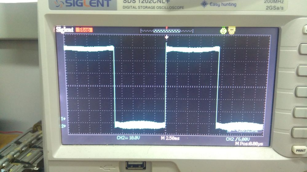
Parts are driven in unipolar modulation mode: HIN1, LIN1 are driven with 23.1 kHz square-wave signals (dead-time 1 us) which represent sine wave signal as their duty cycle is proportional to sinus amplitude (lets call it HF part). HIN2, LIN2 are driven with 10...100 Hz simple square-wave (lets call it LF part), the load is connected to OUT1-OUT2 with filter (3 mH, 3 uF) and the output is sine-wave signal with frequency of LF signal.
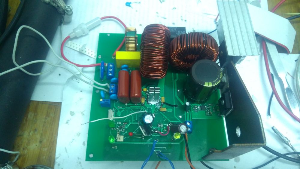
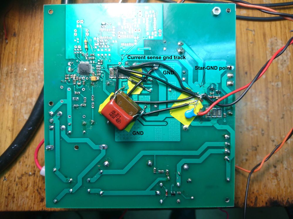
VS=60V, impulse amplitude at inputs of PWD13F60 is 5V, VCC=15V, the PCB is shown below (APFC is at the right and is in OFF state, VS was taken from lab power supply).
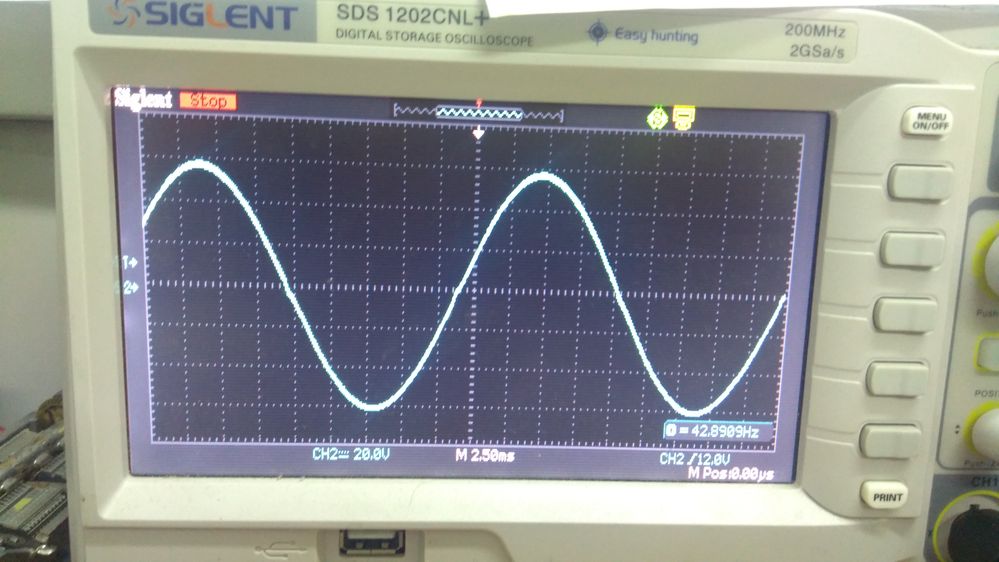
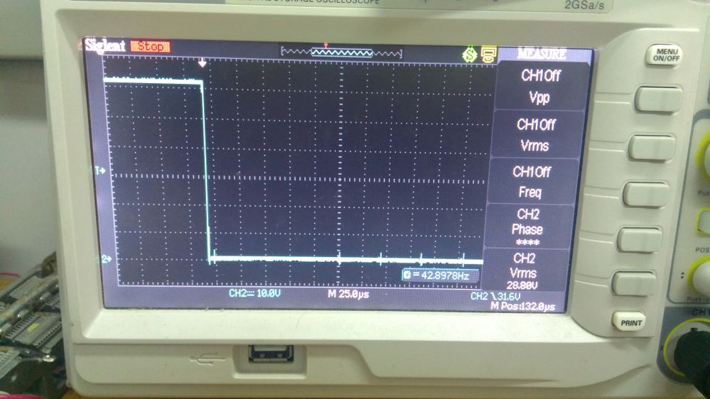
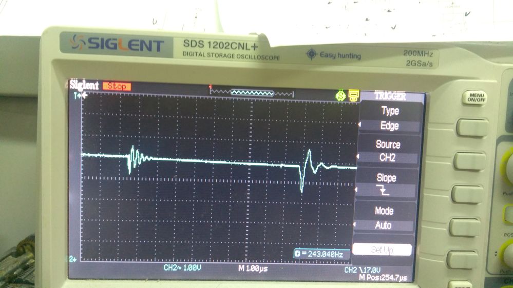
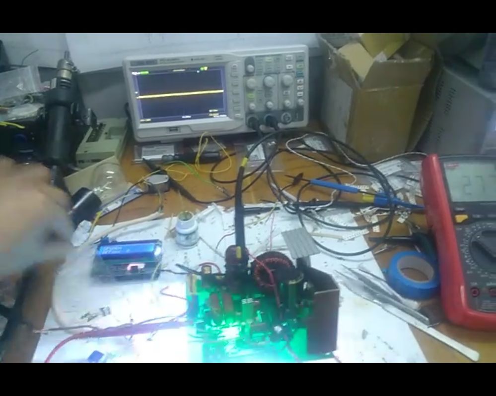
While measuring there is repeating interference at LF impulse with frequency of HF switching and its amplitude is dependent from VS, so at some VS value this interference become so huge that it opens LF part FET while it needs to be closed (!!!) and I have overcurrent protection enabling.
zoomed:
impulses:
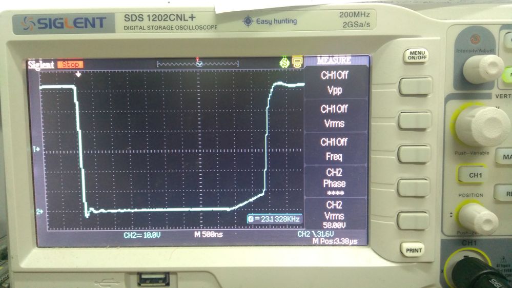
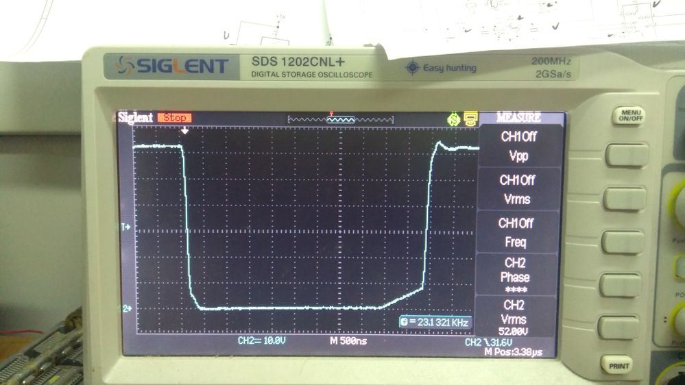
And waveform of HF signals are suitable as for "upper FET" and for "lower FET" as can be seen:
My question is:
Can it be because of inner intercoupling capacitance of IC or I need to modify my PCB and maybe add LPF to LF inputs of PWD13F60 IC? Do I need to use maybe full GND polygon under IC or there is some addition hints.
I have read about distances of 1.2mm between VS and other pads and will remake layout (was 1,05.....1,15mm) so is it need to remake something else. Or the whole PCB?:)
Thank you in advance!
P.S. The case temperature was about 60 C under 0.9A load and 60V VS and also dependent from VS value (VS=30V, 0.9A and only 45 deg temperature). Charge dissipation increase???
- Labels:
-
Motor Control Hardware
- Mark as New
- Bookmark
- Subscribe
- Mute
- Subscribe to RSS Feed
- Permalink
- Email to a Friend
- Report Inappropriate Content
2019-02-13 4:27 AM
Dear Johny,
there is no significant capacitance between the two half bridges due to package.
Based on the info, the application seems using a shunt resistor for overcurrent.
If the GND-shunt-SENSE path is long (inductive), one half bridge could influence the other while operating. Or if input lines are coupled to OUT nodes, them could be too noisy and turning off MOSFETs.
To minimize bus ringing, noise and mutual interference we recommend doing the following:
- keeping short the power decoupling loop: VS-cap-GND-shunt-SENSE. The GND-shunt-SENSE path is the most important
- To minimize the GND-shunt-SENSE path while using a shunt resistor, it is often useful to split the shunt resistor into two resistors. This will lead to have very short GND1-shunt-SENSE1 and GND2-shunt-SENSE2 paths. Examples are EVALPWD13F60 (4 layer) and EVALPWD5F60 (4 layer)
- Using (adding) two small ceramic capacitors, one between VS and GND1 and one between VS and GND2 give the best results in limiting bus spikes and EMI.
To avoid input traces being interfered by OUT nodes, input traces should minimize the coupling to OUT traces by minimizing PCB overlap or by shielding by GND plane. However, it is worth adding at least the footprint for input filtering capacitors in case of residual noise.
The bootstrap capacitor shall be placed between BOOT and OUT pin. It is recommended to use a dedicated trace connecting directly on OUT pad, not far from the device.
Clearance distance between high voltage nets is a general PCB rule to avoid possible arcing but, if the maximum supply voltage is low, clearance distance could be reduced.
23.1 kHz switching frequency is not so low, and switching losses are consequently relevant. Reducing switching frequency should reduce dissipation.
Hard switching commutations losses are voltage dependent (due to diode recovery Qrr, MOSFET intrinsic capacitance Coss and load parasitic capacitance), so it is normal dissipation increases with bus supply voltage.
- Mark as New
- Bookmark
- Subscribe
- Mute
- Subscribe to RSS Feed
- Permalink
- Email to a Friend
- Report Inappropriate Content
2019-02-15 4:33 AM
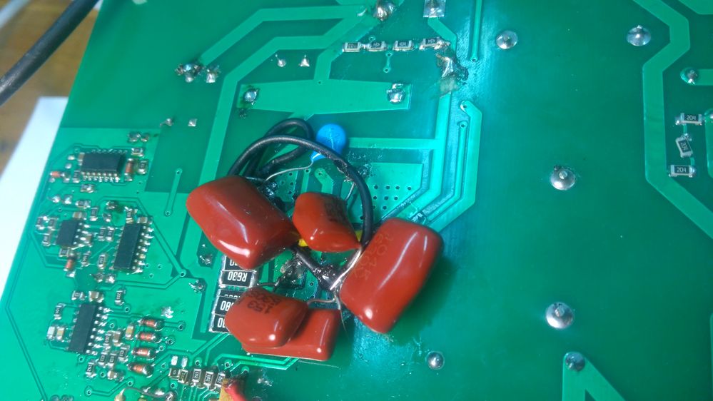
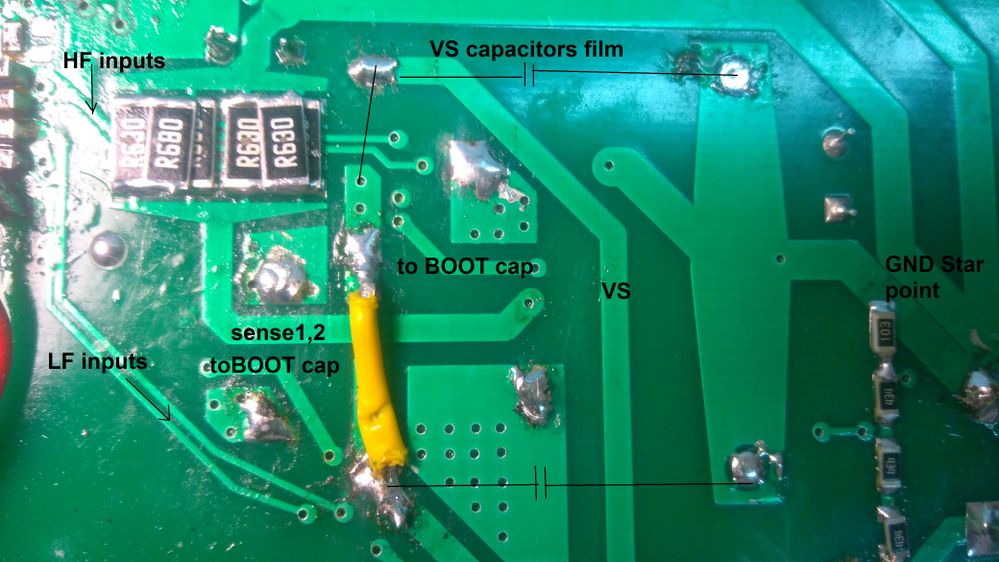
Dear Fabio, thank you for such a detailed answer. We are working on new PCB layout now, because (as we noticed) our old PCB design caused such an interference. Below is “stabilization circuit�? which helped to lower interference on LF bottom part signal. It consists of many:) capacitances soldered directly between OUT1,2 and GND1,2 and VS. So I think the problem is in my PCB.
About the traces. Based on your answer I think that my SENSE circuit design is not suitable also with long Lin1,2 and HIN1,2 traces as shown below.
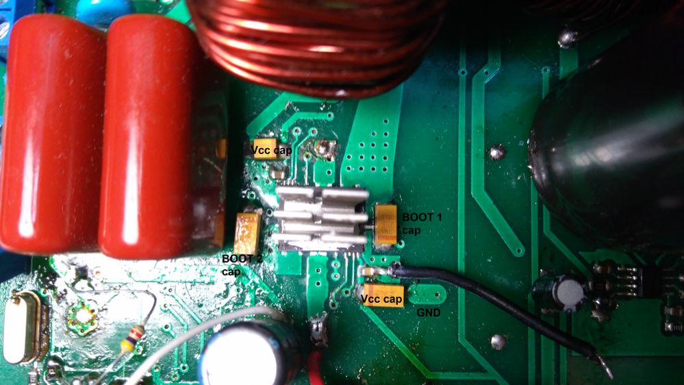
Would it be better for PCB design to make a full GND poly under PWD13F60 with vias to top layer for connecting Vcc caps? Do I need to make dedicated GND trace for PWD13F60 inputs? If I spit SENSE res into 2, so I need to use 2 opamps (comparators)? It can make PCB layout easier.
Is my TOP layout optimal (shown below)?
Would it be better to make VS path wider or polygon GND together with wide OUTs can give much better result?
Thank you in advance!
- Mark as New
- Bookmark
- Subscribe
- Mute
- Subscribe to RSS Feed
- Permalink
- Email to a Friend
- Report Inappropriate Content
2019-02-20 9:40 AM
Dear Johny,
the lenght of LIN and HIN trace does not matter so much. Those signals could be affected mainly if traces runs above/below OUT traces running on other layers. A second reason could be a very noisy GND plane due to porely routed power traces vs signal line traces.
VCC, LIN and HIN caps (I recommend using ceramic capacitors, are normally cheaper and smaller) shall be placed near pins and connect to the related GND (place VCC1 capacitor near VCC1 and GND1 pins, etc).
Also for bootstrap, small (around 100-220nF) ceramic capacitor could, most of the times, fit the application.
How many layers is your PCB? In general, a full GND copper plane can easy layout, but depends on your PCB constraints. Please take a view on the two evaluation boards layout.
Regarding the two sense resistor, you can still short them together as done in the eval board or apply a different strategy as you prefere and depending on your controlling strategy.
If you have thermal issues, you should maximize OUT and VS copper planes to cool down those exposed pads. Since VS is in the middle of the device, could be likely the hotter and shall be preferred for cooling. GND exposed pads are in most of applications relatively cold.
- Mark as New
- Bookmark
- Subscribe
- Mute
- Subscribe to RSS Feed
- Permalink
- Email to a Friend
- Report Inappropriate Content
2019-02-25 7:39 AM
Dear Fabio, thank you for your answer.
As for my experiment, I can say that I've already damaged PWD13F60 at my new PCB:) And need your helpful answers again.
For bootstrap capacitors: I calculated their values for HF and LF parts separately by formula C>2(2Q_gate+I/f+Qiss)*(1/(Vcc-Vfd)) as it done in general for those high-side drivers for bootstrap structure. I obtain something like 0.68uF for HF part and 8uF for LF part, so I used 10uF and 47uF for more reliabilty.
I've incorporated RC-filter at LIN and HIN inputs of 50-HZ branch (110 Ohm, 160 pF) and made wider polygons under GND pads at bottom PCB layer. And it again gets noisy! I tested with 100 V VS with 0.9A resistive load (near 70V_AC_rms_out at 75 Ohm load resistor). I realised my mistake in GND layout! My star-GND point is at "-" pin of PFC output capacitor and GND1 as well as GND2 pads and current-sense resistor gnd pin were led to that star-GND point. So I have very long dedicated traces between GND1, GND2 and current-sense resistor. So it was all noisy.
I connected GND with more wires together with current-sense GND pin to star-GND point and I get much lower noise, so at first, my PCB needs to be re-designed. It's 2-layer PCB.
But when I connected 8200pF mica capacitor between OUT1 and OUT2 directly - the noise almost aboslutely disappeared! My inverter worked for hours with 100V VS and 70 V_AC_out under 0.9 A_out_rms current with case temperature not more than 55 C deg. Victory!:)
Then I wanted to increase VS up to 310 V and use 220V 60W incandescent lamp as a load. My IC has soft-start during first 3 sec of operating (smooth increasing of PWM duty-cycle up to obtain working output rms voltage), so I turned off over-current protection as it wasn't operate in previous experiments with lower VS and everything was good (I think, it was my mistake:)).
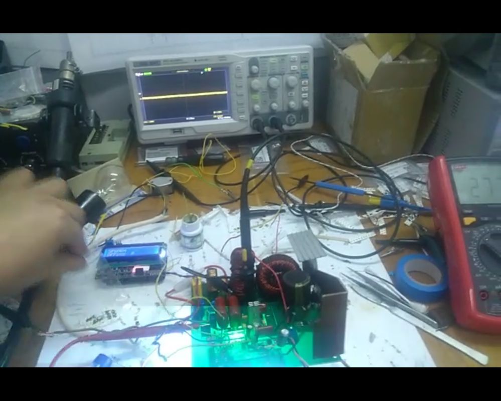
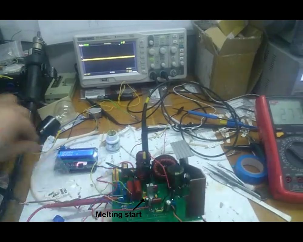
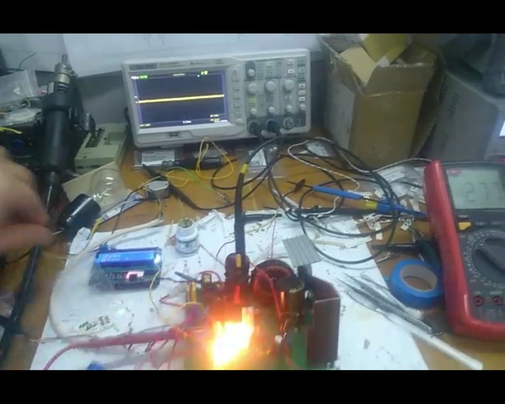
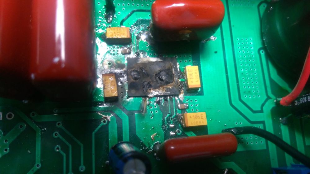
I used 277 V VS and when I turned ON my control IC, PWD13F60 burst in the flame! But control IC works good and RC-filters are not damaged.
As can be seen on screenshots, at first we obtain overheating of current-sense resistors at the bottom layer and then BOOM of PWD13F60.
So I have questions again:
1) Can it be because the absence of over-current protection in case of cold load lamp filament with its low resistance and my soft-start haven't heat it from cold state? But it works good with resistive load that has constant resistance and soft-sart works good too, without over-current protection.
2) Why 8200 pF between OUT1 and OUT2 helps to minimise interference and noise? At my working PWM frequency of 23100 Hz with 390Vdc it will be 0.46A of additional current (if not taking into consideration changes in PWM duty cycle that can lower that current).
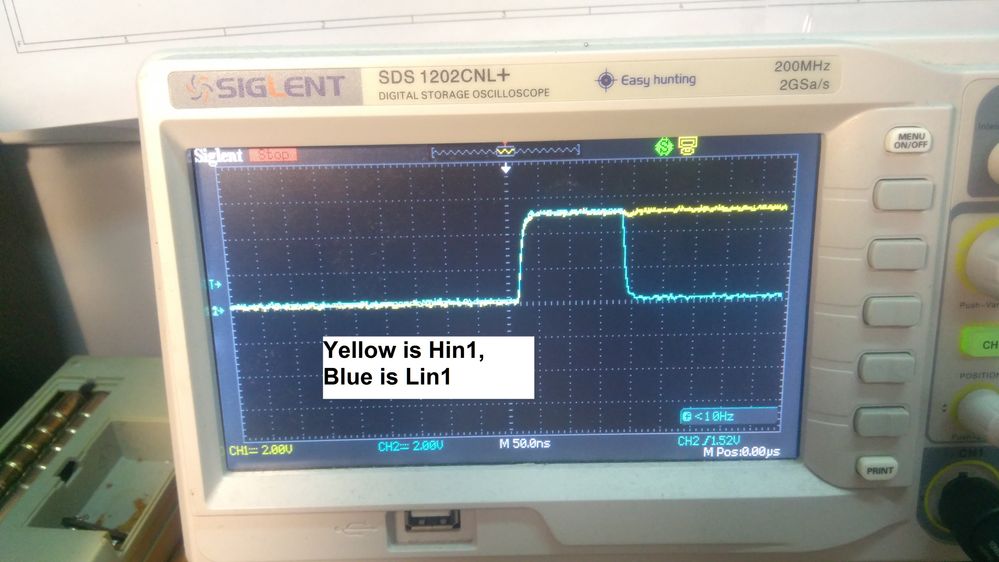
3) My control IC has "a little bug": at start it provide short through-current, for about 170ns.
I know about interlocking feature, but what is its speed? Can PWD13F60 be damaged in case of this short overcurrent? If so, why it wasn't damaged with resistor load?
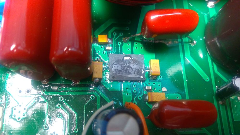
Here is the photo of 2 my damaged PWD13F60:
The first one was used in the first experiment (as I wrote in starting meaasge) with overcurrent protection enabled but with noisy input signals. The second was damaged because of overcurrent (I think). What can you say about the damaging properties if those PWD13F60?
Thank you very-very much!
