Turn on suggestions
Auto-suggest helps you quickly narrow down your search results by suggesting possible matches as you type.
Showing results for
- STMicroelectronics Community
- Product forums
- Power management
- L6902 component choice
Options
- Subscribe to RSS Feed
- Mark Topic as New
- Mark Topic as Read
- Float this Topic for Current User
- Bookmark
- Subscribe
- Mute
- Printer Friendly Page
L6902 component choice
Options
- Mark as New
- Bookmark
- Subscribe
- Mute
- Subscribe to RSS Feed
- Permalink
- Email to a Friend
- Report Inappropriate Content
2024-09-03 12:11 PM
Hi, I'm designing a DIY switching power supply around the L6902. Intended output voltage is <22V, input voltage 24V, output current in constant current mode between 0.6 and 0.8A.
My questions:
- the datasheet shows an inductor value of 22uH, is this value independent of output voltage and current? Currently I chose the part SRU1048-220Y, datasheet: https://www.mouser.de/datasheet/2/54/SRU1048-1391431.pdf
- Is the compensation network also independent of output voltage and current?
For neither of the parts I found any further hints in the datasheet, so I thought I'd better ask...
Thanks very much in advance for your help!
Solved! Go to Solution.
Labels:
16 REPLIES 16
Options
- Mark as New
- Bookmark
- Subscribe
- Mute
- Subscribe to RSS Feed
- Permalink
- Email to a Friend
- Report Inappropriate Content
2024-09-04 02:28 PM - edited 2024-09-04 02:30 PM
Options
- Mark as New
- Bookmark
- Subscribe
- Mute
- Subscribe to RSS Feed
- Permalink
- Email to a Friend
- Report Inappropriate Content
2024-09-04 02:47 PM
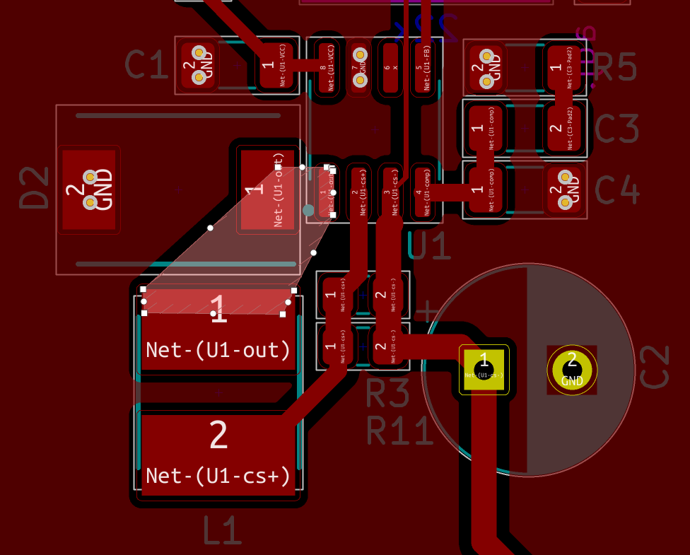
Well, pcb2 has already turned D2 so far that D2.GND has moved quite far away from C2.GND. The same applies to this GND connection: the flowing pulse currents should be able to flow with low impedance between C2 and D2.
pcb3 exacerbates this situation, as D2.GND is moved even further away from C2.
All in all, however, we are already talking about improvements that would have to be implemented for bigger buck regulators converting 20W or more, but which is not quite so critical for your relaxed ~400mW.
So go ahead, use pcb2 and possibly turn C2 90° to the left, which will bring C2.GND a little closer to D2.
In order to give better visibility on the answered topics, please click on Accept as Solution on the reply which solved your issue or answered your question.
Options
- Mark as New
- Bookmark
- Subscribe
- Mute
- Subscribe to RSS Feed
- Permalink
- Email to a Friend
- Report Inappropriate Content
2024-09-04 03:04 PM
Wow, don't you love multi level undo in any software? Despite having everything in a git repo, still so useful... :)
I already imagined that you would criticize the GND point of D2 moving farther away.
I now have a hybrid version with thickened track around pin1 of U1, probably that's the best I can do...
One last question (seems like there's always one more) before I feel I really have to let you have your well deserved rest of the evening, this has turned out to be almost "just in time design review" :grimacing_face:
You talk about 400mW in my design - I presume that's the energy in these peak currents? Because I intent to deliver around 13W DC power with this circuit (21.5V @ 0.6A).
Options
- Mark as New
- Bookmark
- Subscribe
- Mute
- Subscribe to RSS Feed
- Permalink
- Email to a Friend
- Report Inappropriate Content
2024-09-04 11:07 PM
Oops, I accidentally mixed this with another thread, sorry (I shouldn't do everything at the same time).
Your design already looks pretty good. I'm looking forward to the results of the functional test.
Regards
/Peter
In order to give better visibility on the answered topics, please click on Accept as Solution on the reply which solved your issue or answered your question.
Options
- Mark as New
- Bookmark
- Subscribe
- Mute
- Subscribe to RSS Feed
- Permalink
- Email to a Friend
- Report Inappropriate Content
2024-09-05 10:26 AM
I will report back once the project is assembled and tested. Just ordered parts and PCBs...
Options
- Mark as New
- Bookmark
- Subscribe
- Mute
- Subscribe to RSS Feed
- Permalink
- Email to a Friend
- Report Inappropriate Content
2024-09-14 10:57 AM - edited 2024-09-14 11:51 AM
I'm in the process of soldering components. One thing I have noticed is that the IC does not have a very clear pin 1 marking. No dot, no notch. Not very DIY friendly...
Just from datasheet i deducted that the chamfered side has pin one. I'll attach two pictures where I think pin on should be in the upper left corner.
I'll stop for today as I already soldered for more than three hours now. 19 passive components to go and maybe needing to rotate this IC - tomorrow is another day:)
EDIT: I see now from the prcitures that I will have to touch up on the pins with a soldering iron, hot air did not quite do it properly. Will have a full inspection of the board with a magnifying glass after everything is soldered and will touch up as needed. Amazing what a phone camera can do though these days. A microscope is certainly more practical but still...
Options
- Mark as New
- Bookmark
- Subscribe
- Mute
- Subscribe to RSS Feed
- Permalink
- Email to a Friend
- Report Inappropriate Content
2024-09-14 10:32 PM - edited 2024-09-14 11:05 PM
Correct, if the site with the bevelled edge is at the bottom (and as with all IC, if the text is normally legible in front of you), pin 1 is on the bottom left.
In order to give better visibility on the answered topics, please click on Accept as Solution on the reply which solved your issue or answered your question.
- « Previous
-
- 1
- 2
- Next »
Related Content
- Minimum Clock Speed, and enabling PSSI problem in STM32 MCUs Products
- component choice in Interface and connectivity ICs
- Basic questions on getting started with STM32F7 in STM32 MCUs TouchGFX and GUI
- How can I keep component choices fixed when changing the load specs for LED driver simulations? in Others: hardware and software