Turn on suggestions
Auto-suggest helps you quickly narrow down your search results by suggesting possible matches as you type.
Showing results for
- STMicroelectronics Community
- Product forums
- Power management
- Re: L6470 / L6472 VREG line question
Options
- Subscribe to RSS Feed
- Mark Topic as New
- Mark Topic as Read
- Float this Topic for Current User
- Bookmark
- Subscribe
- Mute
- Printer Friendly Page
L6470 / L6472 VREG line question
Options
- Mark as New
- Bookmark
- Subscribe
- Mute
- Subscribe to RSS Feed
- Permalink
- Email to a Friend
- Report Inappropriate Content
2019-06-07 12:25 PM
Hello,
I am designing the system with both L6470PD and L6472PD stepper drivers. Since my system is operating on 3.3V (MCU is STM32F103 ) I have tight the VReg with VDD line as suggested. The problem which I am facing is following. I supply the drivers from 48V while the MCU via DC/DC converter from 24V to 3.3V. If I am turning of the 24V only the logic is still supplied via VREG embedded in Stepper driver ( since 3.3V line is tight with Vreg ). This condition is not good for my application since a) ST not recommended to supply anything from this VREG b) I wanted to be able to turn of the logic completely when I turn on the 24V.
Please advice since it is not clear for me, can I maybe place the Schottky diode between VDD and VReg so there will be no possible supply the system from Vreg?
Or maybe I can leave open the Vreg and not tight this to VDD
Any suggestion is more than great.
Thank you very much
Jacek
Labels:
- Labels:
-
Motor Control Hardware
13 REPLIES 13
Options
- Mark as New
- Bookmark
- Subscribe
- Mute
- Subscribe to RSS Feed
- Permalink
- Email to a Friend
- Report Inappropriate Content
2019-06-10 1:15 PM
Bryan,
No problem Mondays are almost always a bit hectic. You know maybe I will do a bit different approach, I will use the LVD from MCU. If I am seeing voltage below 3.0V it will means that I 24V is out so I will place MCU in the idle state , if the voltage is above 3.3V will means that everything is great and lest rock and roll.
series FET are good idea but it is a extra cost the same like with Schottky diode.
Thanks a lot
Jacek Pieczaba
Options
- Mark as New
- Bookmark
- Subscribe
- Mute
- Subscribe to RSS Feed
- Permalink
- Email to a Friend
- Report Inappropriate Content
2019-08-10 5:33 AM
Bryan,
Just to keep you updated. I was running some tests and it looks that if I simply disconnected from the 3.3V rail the VREG pin.
Thank you
Jacek
Options
- Mark as New
- Bookmark
- Subscribe
- Mute
- Subscribe to RSS Feed
- Permalink
- Email to a Friend
- Report Inappropriate Content
2020-01-13 12:18 PM
Hello Folks
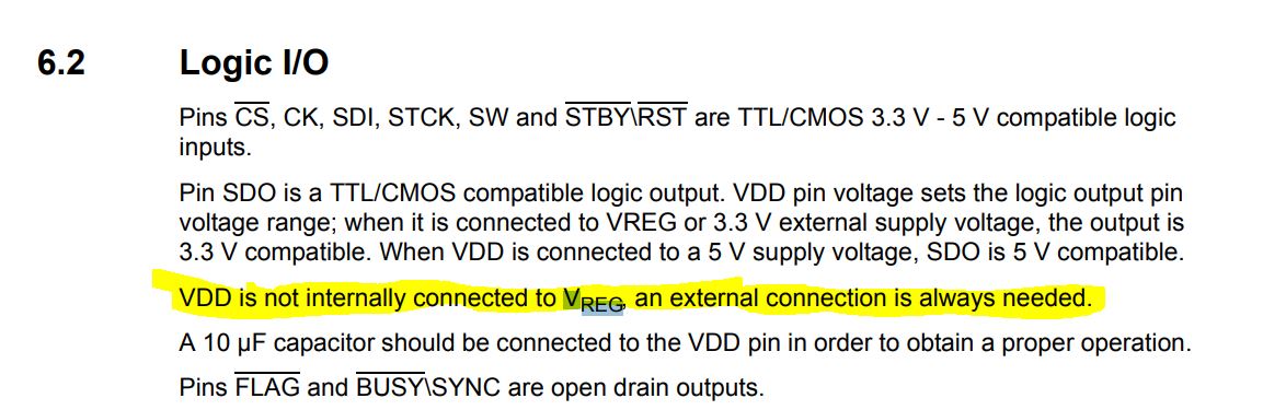
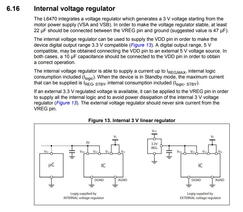
The L6470 datasheet (see snapshots provided by Jacek) clearly says that Vreg should be connected to VDD, as they are not connected internally. Further, VDD should have 10uF Cap to work properly.
Surprisingly, the X-NUCLEO-IHM02A1, which has two of these chip in daisy-chain mode, never connects VDD with Vreg, and there is no 10uF Cap on VDD, and VDD is connected via external power supply. That's fine. However, datasheet says that Vdd and Vreg can be tied all together with external power supply. I have yet to see a schematic by ST where that has been implemented.
On another side, EVAL6470PD schematic also connects Vreg and Vdd of one single L6470PD. That seems to be one of the method prescribed by datasheet. However, it's not mentioned or clarified that can we have both Vdd and Vreg connects to external 3.3V power supply in case of multiple L6470 are used?
My application requires daisy chaining of four L6470PD devices.
Now, my Question is if I have multiple L6470PDs then may I still connect VDD with Vreg? May I have all the Vdds and Vregs of all the L6470 CHIPs tied together and then connect them with external 3.3V supply? Is that fine? or shall I strictly follow the schematic X-NUCLEO-IHM02A1 for multiple L6470?
I have designed a PCB by following design suggestions provided by datsheet. However, it never works properly. The driver behaves erratically as it has mind of its own.
The datasheet is not at all aligned with schematic attached of X-NUCLEO-IHM02A1. I am bamboozled right now. A serious help is required!!
FYI, please see the attached schematic of X-NUCLEO-IHM02A1 and my attached schematic snapshot below for your reference:

Options
- Mark as New
- Bookmark
- Subscribe
- Mute
- Subscribe to RSS Feed
- Permalink
- Email to a Friend
- Report Inappropriate Content
2020-01-15 5:55 AM
Hello JSang.1
Thanks a lot for sharing this with community and maybe I can try to help you. First I had a pleasure to see your schematic and I found two problems which might give you "erratic" behavior of the Chips.
- SPI bus

Both L6470 share the same SPI bus so SDO/SDI/CK lines need to be shared in the same way with both chips CS - chip select should be pin which allow your control unit to pick which one you wanted to activate. So I am seeing that CS line is not individual for each chip , and also the there is so net mismatch for SDO and SDI lines.
- The STBY/RST | Sync_X1 and Flag_X1 lines you pulled up to different voltage that VDD. So since I don't see the full circuit and your final solution if want like tat then the VDD lines need to be tight this VDD_01 and VDD_02 respectively. However if you supply both chips from the same 3.3V bus then VDD_01 and VDD_02 in my opinion should be on the same level.

Now let me explain what I have learned about VDD and VREG. So This L6470 internally contain 3V regulator and it output is present on the VREG pin. If you tight it with the VDD you need to remember about one important mechanism which I was not aware at the beginning. If you generate your 3.3V from different power supply which supply for example your MCU , stepper motor driver etc... , remember that VREG 3V signal in present when you supply the chip with the voltage which you plan to use to supply stepper motor. So in other words if you keep them connected and you disconnect the 3.3V line for you MCU and driver , but the 24V will be still present then because you have VDD and VREG together you will still back feed your MCU with 3V signal. This is not recommended from ST to use VREG line to supply. What I did I am simply disconnected them and add the bypass caps to keep nice stabilization for the internal Vreg (see below ). Now it I disconnect 3.3V line my logic system is turned off even if 24V line is present on the Stepper driver.

So if you don't mind I was adding some modification on your schematic to present suggestions ( schematic is worth 1000 words )
ps. Please add some more capacitors for all VSA and VSB pairs...
I hope my explanation make sense and ask more if you needed I will be more than happy to help.
With Best Regards.
Jacek Pieczaba
- « Previous
-
- 1
- 2
- Next »
Related Content
- L6470 Stepper Driver - Large cap on VS to ground destroyed?? in STM32 MCUs Motor control
- L6470 Different angular speed on stepper motors using RUN command in Power management
- Question about speed profiles for a L6470 in Power management
- L6470 and L6472 - What sets the speed of MOVE and GOTO operations? Using MAX_SPEED parameter imposes lower limit of 15.25 FS/sec and 15.25 FS/sec granularity. in Power management
- Can not set L6470 register in Power management