- STMicroelectronics Community
- Product forums
- Power management
- Re: I am having trouble getting two of the EVALMas...
- Subscribe to RSS Feed
- Mark Topic as New
- Mark Topic as Read
- Float this Topic for Current User
- Bookmark
- Subscribe
- Mute
- Printer Friendly Page
I am having trouble getting two of the EVALMasterGAN1 evaluation boards to properly work in a full bridge configuration. Can someone help with any suggestions to fix the problem I am having?
- Mark as New
- Bookmark
- Subscribe
- Mute
- Subscribe to RSS Feed
- Permalink
- Email to a Friend
- Report Inappropriate Content
2020-10-16 12:15 PM
So far, the boards are working correctly up until the Bus voltage reaches around 130Vin. Then, when monitoring the gate signals on the board at the GH and GL pin on the MasterGAN, the high side of one of the boards seems to not switch correctly anymore. The low side is switching just fine (so out of the 4 gate signals of the 2 EVAL boards, 1 of them stops working correctly). I have tried adding more bootstrap capacitance to the EVAL board, but that doesn't seem to work. Is there a certain amount of power that the internal bootstrap diode can handle, and we need to add an external one, or is there another problem?
Solved! Go to Solution.
- Labels:
-
Motor Control Hardware
Accepted Solutions
- Mark as New
- Bookmark
- Subscribe
- Mute
- Subscribe to RSS Feed
- Permalink
- Email to a Friend
- Report Inappropriate Content
2020-11-18 07:09 AM
Hello @PHenr.1,
The issue seems to be related to a below-ground voltage (BGV) phenomenon experienced by the OUT pins.
Electrically, the OUT pin could safely tolerate even many volts below ground without problems, but the BOOT pin, which is indirectly bound to the OUT pin voltage, cannot.
As reported in the MASTERGAN datasheet (Table 3 Recommended operating conditions) a minimum BOOT voltage (versus GND) is recommended during high-side turn on to allow a proper GaN power transistor turn-on.
Increasing the bus voltage the BGV phenomenon is accentuated, adding external diode you are clamping the maximum negative voltage and keeping the BOOT voltage inside a proper operative range.
Please click on the 'Select as Best' button if my reply fully answered your question.
- Mark as New
- Bookmark
- Subscribe
- Mute
- Subscribe to RSS Feed
- Permalink
- Email to a Friend
- Report Inappropriate Content
2020-11-04 04:47 AM
Hello @PHenr.1 welcome to the ST Community.
Please could you share more details on your application?
- How did you connect the two boards?
- How are you monitoring the GL and GH signals? Which kind of probes are you using and where exactly on the board are you connecting them?
- How are you generating PWM driving signals and at what frequency?
If you have some oscilloscope waveforms please share them.
With these additional info, we try to help you.
- Mark as New
- Bookmark
- Subscribe
- Mute
- Subscribe to RSS Feed
- Permalink
- Email to a Friend
- Report Inappropriate Content
2020-11-04 08:02 AM
Hello,
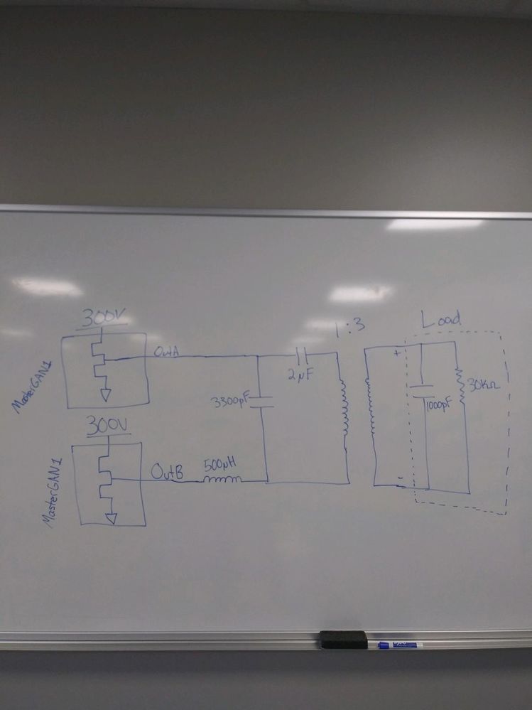
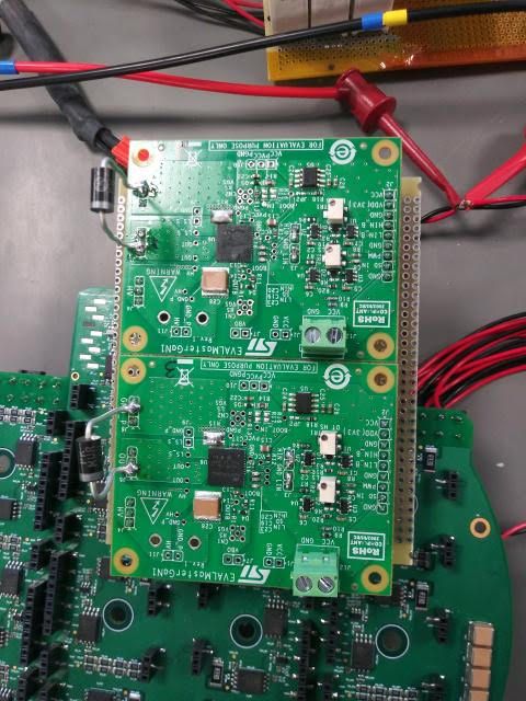
1. We have the 2 boards set up in a full bridge configuration (see attached picture for schematic details)
2. I was monitoring the GH and GL signals with low voltage differential probes at the CN1 and CN2 connectors with the BNC connectors removed
3. The switching frequency is 250kHz and we are generating the PWM signal using known good FPGA code for full bridge configuration, and we are using the high side signal as the PWM signal input and the EVAL board makes the low side signal
We were able to fix the problem using a negative clamping diode on both of the switch nodes, but we were wondering if you have ever seen this problem in the past. If there is another way of fixing our problem without adding external components, then we are up for suggestions.
Patrick Henry
[Edit: do not publish personal info]
- Mark as New
- Bookmark
- Subscribe
- Mute
- Subscribe to RSS Feed
- Permalink
- Email to a Friend
- Report Inappropriate Content
2020-11-04 11:35 PM
Hello @PHenr.1
the picture is missing ;)
Please remember not to publish confidential info, thanks
- Mark as New
- Bookmark
- Subscribe
- Mute
- Subscribe to RSS Feed
- Permalink
- Email to a Friend
- Report Inappropriate Content
2020-11-05 05:32 AM
Hello,
1. We have the 2 boards set up in a full bridge configuration (see attached picture for schematic details)
2. I was monitoring the GH and GL signals with low voltage differential probes at the CN1 and CN2 connectors with the BNC connectors removed
3. The switching frequency is 250kHz and we are generating the PWM signal using known good FPGA code for full bridge configuration, and we are using the high side signal as the PWM signal input and the EVAL board makes the low side signal
We were able to fix the problem using a negative clamping diode on both of the switch nodes, but we were wondering if you have ever seen this problem in the past. If there is another way of fixing our problem without adding external components, then we are up for suggestions.
- Mark as New
- Bookmark
- Subscribe
- Mute
- Subscribe to RSS Feed
- Permalink
- Email to a Friend
- Report Inappropriate Content
2020-11-18 07:09 AM
Hello @PHenr.1,
The issue seems to be related to a below-ground voltage (BGV) phenomenon experienced by the OUT pins.
Electrically, the OUT pin could safely tolerate even many volts below ground without problems, but the BOOT pin, which is indirectly bound to the OUT pin voltage, cannot.
As reported in the MASTERGAN datasheet (Table 3 Recommended operating conditions) a minimum BOOT voltage (versus GND) is recommended during high-side turn on to allow a proper GaN power transistor turn-on.
Increasing the bus voltage the BGV phenomenon is accentuated, adding external diode you are clamping the maximum negative voltage and keeping the BOOT voltage inside a proper operative range.
Please click on the 'Select as Best' button if my reply fully answered your question.
- NUCLEO-H7S3L8 SPI Transmission Issue - TXDR Register Not Updating in STM32 MCUs Products
- Implementing STM32L4S5ZIT6 Bootloader with a Memory Marker in STM32 MCUs Products
- STM32U585OIY6QTR vss_smps directly connect to vss may cause I2C issue? in STM32 MCUs Products
- NUCLEO-H563ZI Uart3 cannot receive more than 2 characters in STM32 MCUs Embedded software
- STM32WL5 Design review in STM32 MCUs Wireless

