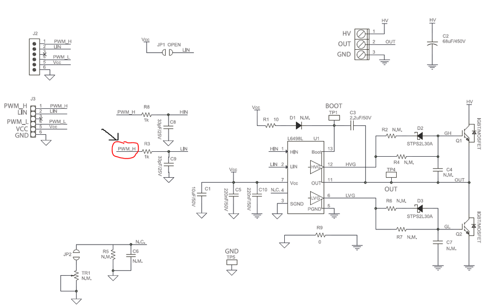
EVAL6498L - how to connect it to the microcontroller?
- Mark as New
- Bookmark
- Subscribe
- Mute
- Subscribe to RSS Feed
- Permalink
- Email to a Friend
- Report Inappropriate Content
2021-02-24 9:13 PM
Hi there, I am a first time user of the gate driver evaluation board EVAL6498L, and I am trying to understand how to connect it to the controller and to the MOSFETs, I am using this document .
Assume I am sending 2 PWM signals from a microcontroller PWM1 and PWM2, where do I connect them? My understanding from your document is that PWM1 must go to the pin 1 of the driver IC and PWM2 to pin 2 of the driver IC, and the controller ground goes to pin 3 of the driver IC.
1) My question is how are these IC pins mapped on the connector J2 of EVAL6498L? My guess is that PWM1 goes to J2-1 and PWM2 goes to J2-4, and the controller ground to J2-6. Would this be correct? Then if this is the case, what is the function of J2-2 (LIN)?
2) I have marked also a part in the drawing, where I am not sure about the label I circled in red. Should that be
PWM_L? (and not PWM_H)? I am a bit confused.
3) is it ok to connect the ground of the Vcc power supply together with the microcontroller ground, in J2-6?
Thank you very much
Lello
Solved! Go to Solution.
- Labels:
-
Motor Control Hardware
Accepted Solutions
- Mark as New
- Bookmark
- Subscribe
- Mute
- Subscribe to RSS Feed
- Permalink
- Email to a Friend
- Report Inappropriate Content
2021-02-25 1:59 AM
Hello @Lello and welcome to the ST Community.
Assuming the abovementioned connections:
- PWM1 connected to the pin1 HIN: high-side driver logic input (active high)
- PWM2 connected to the pin2 LIN: low-side driver logic input (active high)
- Controller ground connected to pin3 SGND: Signal ground.
1) Right, you can apply the PWM1 to J2-1, PWM2 to J2-4, and the controller ground to J2-6.
The J2-2 LIN signal (direct connection to the IC pin without filter network) is available because the same PCB is compatible with the device L6494 (in this IC the pin 2 is the SD line).
2) The drawing is not present, but I think you are referring to the label close to the R3 resistor.
In this case, thank you for signaling, I updated the schematic and planned the documents update on the st.com.
Refer to the attached schematic.
3) Yes, the Vcc supply ground must be connected to J2-6 pin together the microcontroller ground.
Let me know if these info are useful to you, if yes please "Select as Best" button to close the topic.
- Mark as New
- Bookmark
- Subscribe
- Mute
- Subscribe to RSS Feed
- Permalink
- Email to a Friend
- Report Inappropriate Content
2021-02-25 2:45 PM

thank you for your welcome msg and the prompt response. Your answer helps a lot!
- Re (2): In response to your point (2), I attach the drawing with the old schematic. Yes, as you pointed out, the error was on the label close to R3 resistor.
- Re (1): Great, thank you! I will not be using J2-2 then, since my IC is the 6498L. Just out of interest, why is there an RC filter network on the PWM pins 1 and 2 of the IC, I thought the PMW signals would go straight to the IC. I am planning to use a PWM at 30-40 kHz, and wondering if the R-C netweok has any (negative) effect.
- Re (3): thank you - this is clear.
Thank you
Lello
- Mark as New
- Bookmark
- Subscribe
- Mute
- Subscribe to RSS Feed
- Permalink
- Email to a Friend
- Report Inappropriate Content
2021-02-26 12:03 AM
Hi @Lello ,
the logic input pins can be connected directly to the microcontroller (in this case you can remove the two capacitors C8 and C9).
If the application environment is very noisy and the logic input voltage is low (e.g. 3.3 V), it can be useful to place some small RC network in series with the logic input lines, in order to avoid false input triggering due external noise.
Good luck with you work!