- STMicroelectronics Community
- Product forums
- Interface and connectivity ICs
- STUSB4500, can the GPIO (or attach) pin be used to...
- Subscribe to RSS Feed
- Mark Topic as New
- Mark Topic as Read
- Float this Topic for Current User
- Bookmark
- Subscribe
- Mute
- Printer Friendly Page
STUSB4500, can the GPIO (or attach) pin be used to control a MOSTFET for a different power path
- Mark as New
- Bookmark
- Subscribe
- Mute
- Subscribe to RSS Feed
- Permalink
- Email to a Friend
- Report Inappropriate Content
2020-11-10 06:09 PM
Hey ST
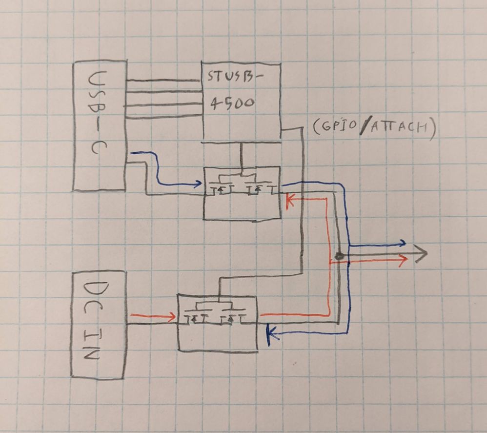
I am building an application that has two power sources, one USB-C (27W) with the STUSB4500 controller, and an optional DC input.
Because the GPIO or attach pins can be open drain, theoretically they could be used to contrl a second FET on the power path of the DC input. Do you guys think the STUSB4500 could handle this?
Also, because the two inputs would be joined, to block revers current, would the STUSB4500 support a back to back FET configuration for the SNK MOSTFET?
The power supply's do not need to be uninterruptible, so switching time is not an issue.
The two power souses will not be present at the same time.
Blue - current path when USB-C cable is plugged in, and sourcing power
Red - current path of DC connector, no USB-C plug present

The on board MCU will use I2C to comunicate with the 4500, if the attach pin could be used to switch the power path of the DC input, that should make is so when a usbc cable is plugged in, the DC input is disabled
Thanks
Jonas
- Mark as New
- Bookmark
- Subscribe
- Mute
- Subscribe to RSS Feed
- Permalink
- Email to a Friend
- Report Inappropriate Content
2020-11-23 05:54 AM
Hello Jonas
Sorry for the late feedback.
I don't think attach/gpio is a good candidate because this is not high voltage GPIO ad thus won't be suitable for your purpose.
I suggest attached schematic to handle 2 power sources. I didn't redraw all stusb4500 application schematic; just to give you an idea.
Best regards
Nathalie
- Mark as New
- Bookmark
- Subscribe
- Mute
- Subscribe to RSS Feed
- Permalink
- Email to a Friend
- Report Inappropriate Content
2020-11-24 04:18 PM
Thanks Nathalie,
Right I missed the high V part of the pin.
That solution looks interesting, just to go over a few points for my understanding,
When DCIN is high (say 9V) that would cause Q1 to pull the gates low, connecting DCIN to VSINK. In this case, R8 would need to over power R4
When VBUS is high (say 9/5V), VBUS_EN_SNK is 0, and DCIN is unconnected, U5 would force the gates high, stopping flow from VSINK to DCIN
If my understanding is correct, R8 should act as a weak pull down, and R4 as a very week pull up?
If U4 allows current to pass from VSINK into drive of Q1, and when VBUS_EN_SNK is 0, there could be a path to GND through (R7+R9)||R8 ?
My understanding is that U3, U4 gates would still be high as U5 would overpower R8 pull down.
Could the drive for Q1 be moved to the DCIN side of U3 to stop the consistent path to GND when VBUS_EN_SNK is 0 and no DCIN is present?
But I may be miss understanding the operation
Thanks for the help
Jonas
- STUSB4761 vs STUSB4700 PD Source for compatibility with STUSB4500 PD Sink in Power management
- STUSB4500 I_SNK_PDO_FLEX in Other: hardware
- STUSB4500 connect to USB type A but The Mosfet it don't actve for get 5v in Other: hardware
- Reading STUSB4500 USB PD status via I2C in Other: hardware
- STUSB4500 damaged during reconnection in Other: hardware