- STMicroelectronics Community
- STM32 MCUs
- STM32 MCUs TouchGFX and GUI
- Strange behavior of the LTDC clock signal at a low...
- Subscribe to RSS Feed
- Mark Topic as New
- Mark Topic as Read
- Float this Topic for Current User
- Bookmark
- Subscribe
- Mute
- Printer Friendly Page
Strange behavior of the LTDC clock signal at a lower voltage
- Mark as New
- Bookmark
- Subscribe
- Mute
- Subscribe to RSS Feed
- Permalink
- Email to a Friend
- Report Inappropriate Content
2019-03-14 03:30 AM
Hi,
I am trying to connect a display which requires a master clock of 27MHz and which operates at 1.8V.
I now have two alternative configurations (both are derived from the code generated by Cube MX). The first configuration is performed by the following code:
void SystemClock_Config(void)
{
  RCC_OscInitTypeDef RCC_OscInitStruct = {0};
  RCC_ClkInitTypeDef RCC_ClkInitStruct = {0};
  RCC_PeriphCLKInitTypeDef PeriphClkInitStruct = {0};

  /**Macro to configure the PLL multiplication factor
  */
  __HAL_RCC_PLL_PLLM_CONFIG(8);
  /**Macro to configure the PLL clock source
  */
  __HAL_RCC_PLL_PLLSOURCE_CONFIG(RCC_PLLSOURCE_HSI);
  /**Configure LSE Drive Capability
  */
  HAL_PWR_EnableBkUpAccess();
  /**Configure the main internal regulator output voltage
  */
  __HAL_RCC_PWR_CLK_ENABLE();
  __HAL_PWR_VOLTAGESCALING_CONFIG(PWR_REGULATOR_VOLTAGE_SCALE3);
  /**Initializes the CPU, AHB and APB busses clocks
  */
  RCC_OscInitStruct.OscillatorType = RCC_OSCILLATORTYPE_HSI;
  RCC_OscInitStruct.HSIState = RCC_HSI_ON;
  RCC_OscInitStruct.HSICalibrationValue = RCC_HSICALIBRATION_DEFAULT;
  RCC_OscInitStruct.PLL.PLLState = RCC_PLL_NONE;
  RCC_OscInitStruct.PLL.PLLSource = RCC_PLLSOURCE_HSI;
  RCC_OscInitStruct.PLL.PLLM = 8;
  if (HAL_RCC_OscConfig(&RCC_OscInitStruct) != HAL_OK)
  {
    Error_Handler();
  }
  /**Initializes the CPU, AHB and APB busses clocks
  */
  RCC_ClkInitStruct.ClockType = RCC_CLOCKTYPE_HCLK|RCC_CLOCKTYPE_SYSCLK
                              |RCC_CLOCKTYPE_PCLK1|RCC_CLOCKTYPE_PCLK2;
  RCC_ClkInitStruct.SYSCLKSource = RCC_SYSCLKSOURCE_HSI;
  RCC_ClkInitStruct.AHBCLKDivider = RCC_SYSCLK_DIV1;
  RCC_ClkInitStruct.APB1CLKDivider = RCC_HCLK_DIV2;
  RCC_ClkInitStruct.APB2CLKDivider = RCC_HCLK_DIV1;

  if (HAL_RCC_ClockConfig(&RCC_ClkInitStruct, FLASH_LATENCY_0) != HAL_OK)
  {
    Error_Handler();
  }
  PeriphClkInitStruct.PeriphClockSelection = RCC_PERIPHCLK_LTDC|RCC_PERIPHCLK_USART3;
  PeriphClkInitStruct.PLLSAI.PLLSAIN = 108;
  PeriphClkInitStruct.PLLSAI.PLLSAIR = 2;
  PeriphClkInitStruct.PLLSAI.PLLSAIQ = 2;
  PeriphClkInitStruct.PLLSAI.PLLSAIP = RCC_PLLSAIP_DIV2;
  PeriphClkInitStruct.PLLSAIDivQ = 1;
  PeriphClkInitStruct.PLLSAIDivR = RCC_PLLSAIDIVR_4;
  PeriphClkInitStruct.Usart3ClockSelection = RCC_USART3CLKSOURCE_HSI;
  if (HAL_RCCEx_PeriphCLKConfig(&PeriphClkInitStruct) != HAL_OK)
  {
    Error_Handler();
  }
}
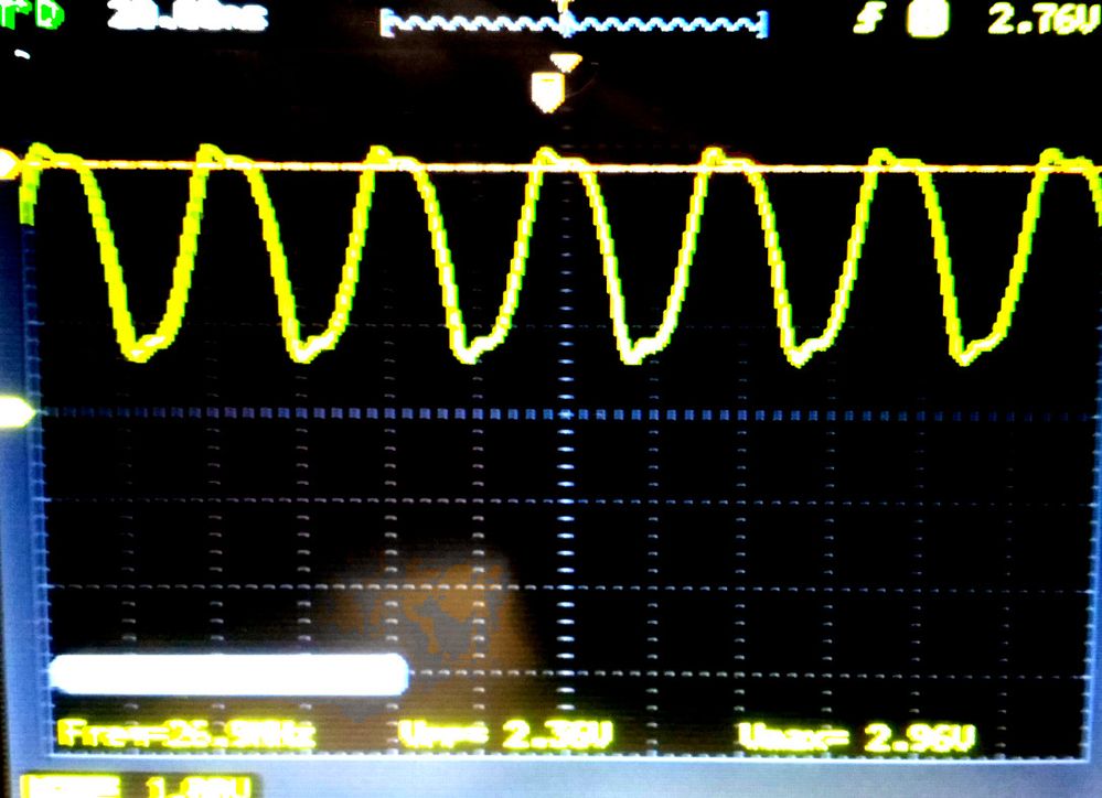
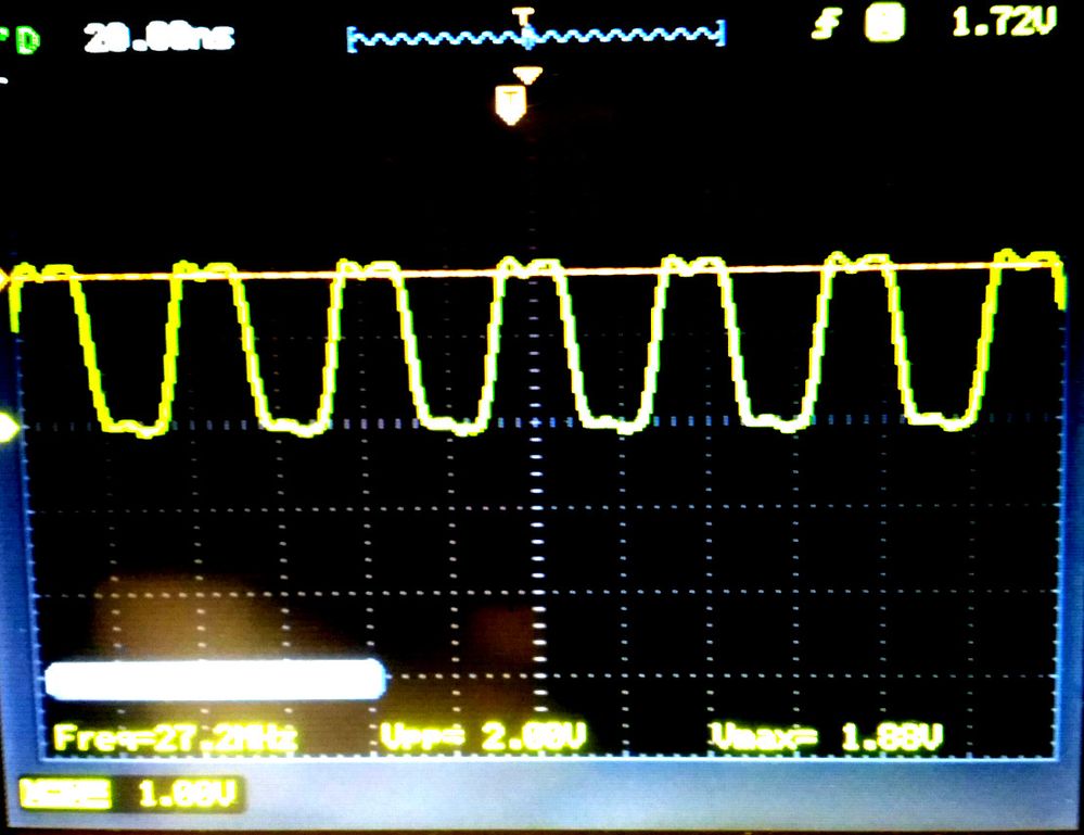
When I check the LTDC clock signal from MCU powered at 3.3V, I get the following output (the clock shape is distorted by my measuring system - I have relatively long cables connected to the NUCLEO board, and the oscilloscope proble is connected to these cables):
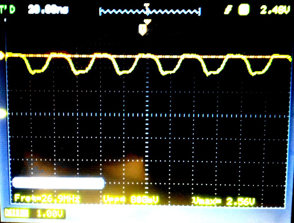
You can see that the signal has around 0.5V offset. As I decrease the input voltage, the offset increases. Here's how it looks for 2.8V (offset around 1.5V):
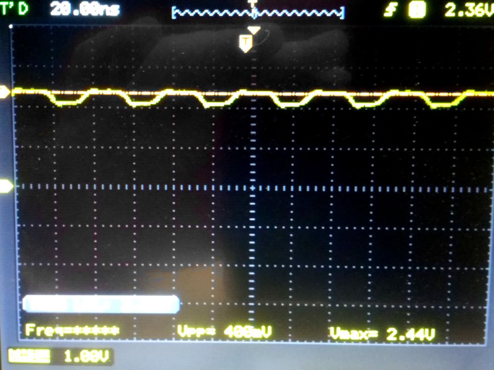
For 2.6V the offset makes the signal look like noise (and for lower voltages it's almost straight out flat):
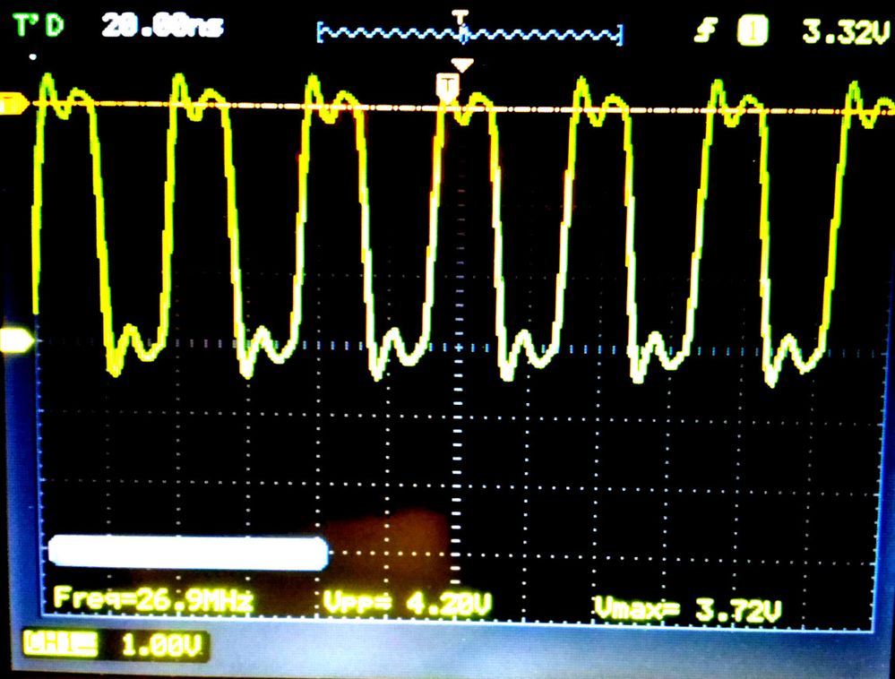
I have another clock configuration, which produces a significantly better signal. At 3.3V it looks like this:
whereas at 1.8V it looks like this:
which is exactly what I want. However, this configuration has an embarrasing side effect, namely that everything else except the clock (UART and all other LTDC signals) stops working.
Here's the clock initialization code to produce this behavior:
__weak void BSP_ClockConfig(void) {

    __HAL_RCC_PLL_PLLM_CONFIG(8);
    __HAL_RCC_PLL_PLLSOURCE_CONFIG(RCC_PLLSOURCE_HSI);
    __HAL_RCC_PWR_CLK_ENABLE();
    __HAL_PWR_VOLTAGESCALING_CONFIG(PWR_REGULATOR_VOLTAGE_SCALE3);
    RCC_OscInitTypeDef RCC_OscInitStruct = {0};

    RCC_OscInitStruct.OscillatorType = RCC_OSCILLATORTYPE_HSI|RCC_OSCILLATORTYPE_LSI;
    RCC_OscInitStruct.HSIState = RCC_HSI_ON;
    RCC_OscInitStruct.HSICalibrationValue = RCC_HSICALIBRATION_DEFAULT;
    RCC_OscInitStruct.LSIState = RCC_LSI_ON;
    RCC_OscInitStruct.PLL.PLLState = RCC_PLL_OFF;
    RCC_OscInitStruct.PLL.PLLSource = RCC_PLLSOURCE_HSI;
    RCC_OscInitStruct.PLL.PLLM = 8;
    HAL_RCC_OscConfig(&RCC_OscInitStruct);

    RCC_ClkInitTypeDef RCC_ClkInitStruct = {0};
    RCC_ClkInitStruct.ClockType = RCC_CLOCKTYPE_HCLK|RCC_CLOCKTYPE_SYSCLK
        |RCC_CLOCKTYPE_PCLK1|RCC_CLOCKTYPE_PCLK2;
    RCC_ClkInitStruct.SYSCLKSource = RCC_SYSCLKSOURCE_HSI;
    RCC_ClkInitStruct.AHBCLKDivider = RCC_SYSCLK_DIV1;
    RCC_ClkInitStruct.APB1CLKDivider = RCC_HCLK_DIV4;
    RCC_ClkInitStruct.APB2CLKDivider = RCC_HCLK_DIV2;

    HAL_RCC_ClockConfig(&RCC_ClkInitStruct, FLASH_LATENCY_0);
    static RCC_PeriphCLKInitTypeDef  periph_clk_init_struct;

    /* SCREEN LCD clock configuration */
    /* PLLSAI_VCO Input = HSE_VALUE/PLL_M = 1 Mhz */
    /* PLLSAI_VCO Output = PLLSAI_VCO Input * PLLSAIN = 192 Mhz */
    /* PLLLCDCLK = PLLSAI_VCO Output/PLLSAIR = 192/5 = 38.4 Mhz */
    /* LTDC clock frequency = PLLLCDCLK / LTDC_PLLSAI_DIVR_4 = 38.4/4 = 9.6Mhz */
    periph_clk_init_struct.PeriphClockSelection = RCC_PERIPHCLK_LTDC | RCC_PERIPHCLK_RTC | RCC_PERIPHCLK_USART3;
    periph_clk_init_struct.PLLSAI.PLLSAIN = 108;
    periph_clk_init_struct.PLLSAI.PLLSAIR = 2; //SCREEN_FREQUENCY_DIVIDER;
    periph_clk_init_struct.PLLSAI.PLLSAIQ = 2;

    periph_clk_init_struct.PLLSAIDivQ = 1;
    periph_clk_init_struct.PLLSAI.PLLSAIP = RCC_PLLSAIP_DIV2;
    periph_clk_init_struct.PLLSAIDivR = RCC_PLLSAIDIVR_4;
    periph_clk_init_struct.RTCClockSelection = RCC_RTCCLKSOURCE_LSI;
    periph_clk_init_struct.Usart3ClockSelection = RCC_USART3CLKSOURCE_HSI;

    HAL_RCCEx_PeriphCLKConfig(&periph_clk_init_struct);
}
Is it possible to get "the best of both worlds" - having a decent clock with no offset and working peripherals?
- STM32H743 standby mode and IWDG only works after power cycle ? in STM32 MCUs Products
- STM32h7 SPI DMA communication issues + FIFO Error (FEIF) in STM32 MCUs Products
- USB damaged (perhaps) after changing biasing source in STM32 MCUs Products
- ADC changes values after voltage change on neighboring channel in STM32 MCUs Products
- STM32 Canbus Multiple Device Weird İssue in STM32 MCUs Embedded software
