Turn on suggestions
Auto-suggest helps you quickly narrow down your search results by suggesting possible matches as you type.
Showing results for
- STMicroelectronics Community
- STM32 MCUs
- STM32 MCUs Security
- 32F417 and RDP2: OTP (512 bytes) and SRAM executio...
Options
- Subscribe to RSS Feed
- Mark Topic as New
- Mark Topic as Read
- Float this Topic for Current User
- Bookmark
- Subscribe
- Mute
- Printer Friendly Page
32F417 and RDP2: OTP (512 bytes) and SRAM execution
Options
- Mark as New
- Bookmark
- Subscribe
- Mute
- Subscribe to RSS Feed
- Permalink
- Email to a Friend
- Report Inappropriate Content
2024-08-21 03:09 AM
This
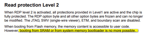
suggests that one cannot execute code from SRAM. Is that really correct?
Also there is ambiguity on whether the OTP area (512 bytes plus the control block) is readable in RDP2. Why say "512 bytes" and not just all-OTP?

The OTP area must remain usable under RDP2 and readable by internal code, but not accessible externally (with a debugger).
Above is from
Solved! Go to Solution.
Labels:
- Labels:
-
STM32 Security
11 REPLIES 11
Options
- Mark as New
- Bookmark
- Subscribe
- Mute
- Subscribe to RSS Feed
- Permalink
- Email to a Friend
- Report Inappropriate Content
2024-08-22 05:30 AM
> Is the code for programming the OTP identical to programming the CPU FLASH?
I believe so. Just with the caveat that it can never be erased, and the addition of the lock byte functionality. If you want to modify less than 32 bits, you can set the other bits to 1 and they won't change as programming flash can only change a bit from 1 -> 0.
If you feel a post has answered your question, please click "Accept as Solution".
Options
- Mark as New
- Bookmark
- Subscribe
- Mute
- Subscribe to RSS Feed
- Permalink
- Email to a Friend
- Report Inappropriate Content
2024-08-22 05:55 AM - edited 2024-08-22 06:01 AM
My reading of the RM text is that you can write the OTP area as much as you like (IOW it is identical to other CPU FLASH) and it becomes non-writable only when the lock byte(s) get set.
But you cannot - even before the locks are set - erase any of it i.e. apply an erase command. Once a bit is 0 you cannot make it 1.
The code I posted above does not do any erase because I am using the block erase (block being 16k to 128k acocrding to where) beforehand.
- « Previous
-
- 1
- 2
- Next »
Related Content
- B-WL5M-SUBG1 LoRa HAL Setup and/or TX Failing in STM32 MCUs Wireless
- Error when installing secure firmware image to STM32U585 in STM32 MCUs Security
- Issue with Programming NOR Flash MT25QL512ABB1EW9 Using STM32H735IGT6 in STM32 MCUs Products
- Debugger's "Step Over" acts incorrectly in STM32 MCUs Products
- memcpy causes NMI fault in H563 in STM32 MCUs Products