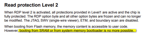
32F417 and RDP2: OTP (512 bytes) and SRAM execution
- Mark as New
- Bookmark
- Subscribe
- Mute
- Subscribe to RSS Feed
- Permalink
- Email to a Friend
- Report Inappropriate Content
2024-08-21 3:09 AM
This
suggests that one cannot execute code from SRAM. Is that really correct?
Also there is ambiguity on whether the OTP area (512 bytes plus the control block) is readable in RDP2. Why say "512 bytes" and not just all-OTP?

The OTP area must remain usable under RDP2 and readable by internal code, but not accessible externally (with a debugger).
Above is from
Solved! Go to Solution.
- Labels:
-
STM32 Security
Accepted Solutions
- Mark as New
- Bookmark
- Subscribe
- Mute
- Subscribe to RSS Feed
- Permalink
- Email to a Friend
- Report Inappropriate Content
2024-08-21 12:38 PM
No. In RDP2, there's no mechanism to interact with the chip anymore outside of user code. Debug interface is disabled, bootloader can't run.
- Mark as New
- Bookmark
- Subscribe
- Mute
- Subscribe to RSS Feed
- Permalink
- Email to a Friend
- Report Inappropriate Content
2024-08-21 5:15 AM
> suggests that one cannot execute code from SRAM. Is that really correct?
It says that you cannot boot from SRAM, which is accurate. You can still run code from SRAM if that's what your flash program does. OTP is readable by your user program in RDP2.
- Mark as New
- Bookmark
- Subscribe
- Mute
- Subscribe to RSS Feed
- Permalink
- Email to a Friend
- Report Inappropriate Content
2024-08-21 5:27 AM
What is "booting from RAM"?
At reset, the CPU goes to the table at VTOR and loads SP and PC from that.
Do you mean that the vector table cannot be RAM-based? I know it cannot be in CCM (because you can't execute code from CCM) but that's a different thing.
- Mark as New
- Bookmark
- Subscribe
- Mute
- Subscribe to RSS Feed
- Permalink
- Email to a Friend
- Report Inappropriate Content
2024-08-21 5:50 AM
> What is "booting from RAM"?
Here are the boot options on the STM32F417:

Booting from SRAM is not a typical configuration.
> Do you mean that the vector table cannot be RAM-based?
No. Hopefully the above table clarifies that.
If you boot from flash, there are no restrictions on placing or executing anything in flash or SRAM.
- Mark as New
- Bookmark
- Subscribe
- Mute
- Subscribe to RSS Feed
- Permalink
- Email to a Friend
- Report Inappropriate Content
2024-08-21 12:03 PM
Is RDP2, is OTP readable in any way apart from code running internally (RAM or FLASH)?
- Mark as New
- Bookmark
- Subscribe
- Mute
- Subscribe to RSS Feed
- Permalink
- Email to a Friend
- Report Inappropriate Content
2024-08-21 12:38 PM
No. In RDP2, there's no mechanism to interact with the chip anymore outside of user code. Debug interface is disabled, bootloader can't run.
- Mark as New
- Bookmark
- Subscribe
- Mute
- Subscribe to RSS Feed
- Permalink
- Email to a Friend
- Report Inappropriate Content
2024-08-21 1:41 PM
Q1: Is there any doc on the initial value of the OTP? I would assume 16 x 32 x 0xFF but the RM does not say that AFAICT.
One could set it to say 0x00 and then lock it.
Q2: what is the easiest way for user code to tell if RDP2 is set? Some registers are not readable.
- Mark as New
- Bookmark
- Subscribe
- Mute
- Subscribe to RSS Feed
- Permalink
- Email to a Friend
- Report Inappropriate Content
2024-08-21 2:52 PM
They're in flash. Erased flash on the STM32F4 is 0xFF. That's certainly in the RM somewhere. The following part of the reference manual lets you infer that 0xFF is the default value, but perhaps it could be more explicit.

Read the value, compare it to 0xCC.

- Mark as New
- Bookmark
- Subscribe
- Mute
- Subscribe to RSS Feed
- Permalink
- Email to a Friend
- Report Inappropriate Content
2024-08-21 3:24 PM
Thank you TDK for those super quick and clear replies!
- Mark as New
- Bookmark
- Subscribe
- Mute
- Subscribe to RSS Feed
- Permalink
- Email to a Friend
- Report Inappropriate Content
2024-08-22 3:21 AM
One more Q:
Is the code for programming the OTP identical to programming the CPU FLASH?
I already have a boot loader which copies itself to RAM and programs the CPU FLASH from there. One has to always do 4 bytes at a time.
There is also lock and unlock, and this is a separate lock and unlock from the OTP ones.
This is the existing code:
/**
  * @brief  Locks the FLASH control register access
  * @retval
  */
static void L_HAL_FLASH_Lock(void)
{
	// Wait for any flash operation to finish
	while(__HAL_FLASH_GET_FLAG(FLASH_FLAG_BSY) != RESET);
	// Set the LOCK Bit to lock the FLASH Registers access
	FLASH->CR |= FLASH_CR_LOCK;
}


/**
  * @brief  Unlock the FLASH control register access
  * Issues the unlok codes
  */

static void L_HAL_FLASH_Unlock(void)
{
	// Wait for any flash operation to finish
	while(__HAL_FLASH_GET_FLAG(FLASH_FLAG_BSY) != RESET);
	// Write the two unlock codes
	WRITE_REG(FLASH->KEYR, FLASH_KEY1);
	WRITE_REG(FLASH->KEYR, FLASH_KEY2);
}


/**
  * @brief  Program word (32-bit) at a specified address.
  * @note   This function must be used when the device voltage range is from
  *         2.7V to 3.6V.
  *
  * @note   If an erase and a program operations are requested simultaneously,
  *         the erase operation is performed before the program one.
  *
  * @PAram  Address specifies the address to be programmed.
  * @PAram  Data specifies the data to be programmed.
  * @retval None
  * Waits for previous operation to finish
  *
  */

static void L_FLASH_Program_Word(uint32_t Address, uint32_t Data)
{
	// wait for any previous op to finish
	while(__HAL_FLASH_GET_FLAG(FLASH_FLAG_BSY) != RESET);
	// clear program size bits
	CLEAR_BIT(FLASH->CR, FLASH_CR_PSIZE);
	// reload program size bits
	FLASH->CR |= FLASH_PSIZE_WORD;
	// enable programming
	FLASH->CR |= FLASH_CR_PG;
	// write the data in
	*(volatile uint32_t*)Address = Data;
}