- STMicroelectronics Community
- STM32 MCUs
- STM32 MCUs Products
- Re: Using J-Link w/Discovery Boards for both F4 an...
- Subscribe to RSS Feed
- Mark Topic as New
- Mark Topic as Read
- Float this Topic for Current User
- Bookmark
- Subscribe
- Mute
- Printer Friendly Page
Using J-Link w/Discovery Boards for both F4 and F0 MCUs
- Mark as New
- Bookmark
- Subscribe
- Mute
- Subscribe to RSS Feed
- Permalink
- Email to a Friend
- Report Inappropriate Content
2012-11-12 9:47 AM
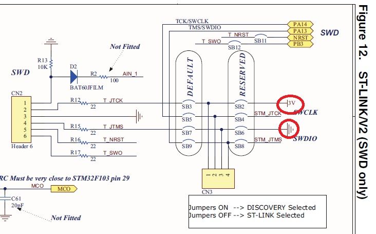
Greetings - Seek the higher performance (faster downloads) achievable w/J-Link ''SWD'' rather than the ''on-board'' ST-Link. Reviewed the F4 Discovery schematic - does not appear that there is any easy way to ''break/open'' SW_CLK and SW_DATA between the STM32F103 ''Link'' and the F4.
CN2 - labeled ''SWD'' appears to be an, ''Output only'' connection. (so that the ST-Link MCU may transfer SWD to an external MCU/board). My goal is to adapt/attach the J-Link @ CN2 - and eliminate any signal contention between the J-Link probe and the F103 ''link'' MCU. Has this been tried/implemented? Search has not uncovered this usage - but I believe that this is a worthwhile objective. Thanks for any guidance you may provide... #f4-discovery- Mark as New
- Bookmark
- Subscribe
- Mute
- Subscribe to RSS Feed
- Permalink
- Email to a Friend
- Report Inappropriate Content
2012-11-12 10:05 AM
Wouldn't the CN3 jumper be a more opportune injection point?
Up vote any posts that you find helpful, it shows what's working..
- Mark as New
- Bookmark
- Subscribe
- Mute
- Subscribe to RSS Feed
- Permalink
- Email to a Friend
- Report Inappropriate Content
2012-11-12 11:23 AM
Thank you - we did see/note CN3 - but as CN2 is both board-edge and labeled SWD - it seemed most appealing.
Issue of breaking the existing SWD signal routing between F103/ST-Link and the M4 remains. Seems overly restrictive to force those who have/use J-Link into a (likely) less capable mode...- Mark as New
- Bookmark
- Subscribe
- Mute
- Subscribe to RSS Feed
- Permalink
- Email to a Friend
- Report Inappropriate Content
2012-11-12 11:44 AM
Isn't the purpose of SB5 and SB9 for disconnecting the on-board ST-LINK?
And for that matter the SB2,4,6,8 pads as an injection point.Up vote any posts that you find helpful, it shows what's working..
- Mark as New
- Bookmark
- Subscribe
- Mute
- Subscribe to RSS Feed
- Permalink
- Email to a Friend
- Report Inappropriate Content
2012-11-12 1:03 PM
Again - thank you. We did check the multi-page schematic - and of course would not have so posted if any F4 ''SWD-only'' ''injection point'' was clear - or even marked as such.
And indeed - just as you say - SB5/9 do appear to route directly to F4 MCU SWD pins. Upper right of Fig 12 shows 4 ''off-page'' port connections ''SWD'' - but failed to label these as going to the F4 MCU, exclusively. (and this is what we missed) Slight disagreement re: SB2,4,6,8 as, ''injection points.'' Our sense is that these route directly & exclusively to the ST Link (F103) - and on reflection they are ''injection points'' from the perspective of the ST Link - but not so from our outside JTAG view-point. So thank you - w/your guidance we can attach modified J-Link ribbon to SB5 & SB9 - along with sigs to SB11 & SB12 - to introduce a more standard JTAG probe into the F4 Discovery board.- Mark as New
- Bookmark
- Subscribe
- Mute
- Subscribe to RSS Feed
- Permalink
- Email to a Friend
- Report Inappropriate Content
2012-11-12 1:12 PM
The apposing sides of the SB having VCC/GND does perplex me, and thus the suggestion it's considered 8 pads rather than purely solder bridges. Or that dropping SB3,5,7,9 and adding SB2,4,6,8 makes CN2 a 4-pin SWD connector?

Up vote any posts that you find helpful, it shows what's working..
- Mark as New
- Bookmark
- Subscribe
- Mute
- Subscribe to RSS Feed
- Permalink
- Email to a Friend
- Report Inappropriate Content
2012-11-12 1:46 PM
Again - great thanks. Agree w/your comments - even futher - Pg 19 of the UM states that SB:2,4,6,8 are Open and SB:3,5,7,9 are Closed - thus how does CN3's short of CN3: 1-2 & CN3: 3-4 ever bring, ''STM JTCK and STM JTMS ''across'' the Open SB4 & SB8? Makes no sense to me...
Another ''impossible'' - just how does STM JTCK ever reach SB3 (so that it flows to CN2-2) with no jumpers employed @ CN3? (same holds for STM JTMS - no clear path is shown for its routing to CN2-4) As you suggest - board implementation is NOT likely to be as shown in this schematic - our original point... Perhaps we are coming closer to agreement - this schematic & manual are confounding in their powers of clear/crisp explanation... We do appreciate & thank you for your interest...- Getting started with STM32 Discovery boards in STM32 MCUs Boards and hardware tools
- STM32F405RGT6 and CAN not working in STM32 MCUs Products
- VFD development boards in STM32 MCUs Boards and hardware tools
- STM32CubeMonitor 1.10 on Windows does NOT start in STM32CubeMonitor (MCUs)
- STM32F446RE CAN Works in Loopback Mode but Not in Normal Mode in STM32 MCUs Products