- STMicroelectronics Community
- STM32 MCUs
- STM32 MCUs Products
- Re: Trouble with 16 bit DMA transfer memory to per...
- Subscribe to RSS Feed
- Mark Topic as New
- Mark Topic as Read
- Float this Topic for Current User
- Bookmark
- Subscribe
- Mute
- Printer Friendly Page
Trouble with 16 bit DMA transfer memory to peripheral
- Mark as New
- Bookmark
- Subscribe
- Mute
- Subscribe to RSS Feed
- Permalink
- Email to a Friend
- Report Inappropriate Content
2018-10-11 1:45 AM
Hello,
I have a strange problem with a 16 bit DMA transfer memory to peripheral on STM32F439, using Nucleo F439ZI.
My goal is to create a sequence of pulses with different pulse widths. I use a timer (TIM2), set its prescaler and set Ch1 to toggle on match with CCR1= 0. Also I generate a DMA request on CC1 event with source = a uint16_t array and destination = TIM2 ARR. ARPE is set. PSIZE and MSIZE are set to half word and it uses direct mode.
So far everything works but my problem is, that pulse lengths are far too much. As much as I found out with debugging ARR is not only loaded with a halfword but both halfwords are loaded with the new value. Eg the current array value the DMA memory pointer points to is 0x12 then ARR is set to 0x00120012, which of course makes the pulse much longer than only 0x12.
What makes this case even more weired is this: there is another option to create these pulses, that is setting ARR to a fixed value and change PSC via DMA. This one works as expected. Maybe it is because PSC uses only 16 bits so it will not bother if the upper half word is written to some value (?)
I want to use the first solution because it has the possibility to set ARR to 0 which will stop the pulse generation. This is not available when setting PSC.
Am I missing something, maybe with DMA settings?
Here is my initialisation code:
uint16_t pulse_data [500] = {2,3,4,5,6,7,8,9,10,11,12,13,14,15,16,17,18,0};


  // reset Timers
  SetBitMask (RCC->APB1RSTR, RCC_APB1RSTR_TIM2RST);
  ClearBitMask (RCC->APB1RSTR, RCC_APB1RSTR_TIM2RST);
  // enable Timer clks:
  SetBitMask (RCC->APB1ENR, RCC_APB1ENR_TIM2EN);
  __DSB ();  // needs to be here according to errata, to wait till periph clk is enabled

  SetBitMask (TIM2->CR1, TIM_CR1_ARPE);
//#define TIM2_prescaler 2.0
//#define TIM2_devider (uint32_t)(APB1_timer_clk_Hz / (2*100000.0)) // Timer tick in Hz
#define TIM2_prescaler (uint32_t)(APB1_timer_clk_Hz / (4*100000.0)) // Timer tick in Hz
#define TIM2_devider 2
  TIM2->PSC = (uint16_t)(TIM2_prescaler) - 1;
  TIM2->ARR = TIM2_devider - 1;
  SetBitMask (TIM2->CCMR1, TIM_CCMR1_OC1PE | TIM_CCMR1_OC1M_1 | TIM_CCMR1_OC1M_0); // Ch1: toggle on match
  TIM2->CCR1 = 0 ; //TIM2_devider - 1;
  SetBitMask (TIM2->CCER, TIM_CCER_CC1E);
  SetBitMask (TIM2->DIER, TIM_DIER_CC1DE);
  SetBitMask (TIM2->CR2, TIM_CR2_MMS_2 ); // | TIM_CR2_CCDS); // OC1Ref to TRGO, DMA req on update

  // load all shadow registers:
  SetBitMask (TIM2->EGR, TIM_EGR_UG);

  // DMA1 init:
  // Stream5 channel3 = TIM2 Ch1
  // reset DMA:
  SetBitMask (RCC->AHB1RSTR, RCC_AHB1RSTR_DMA1RST);
  ClearBitMask (RCC->AHB1RSTR, RCC_AHB1RSTR_DMA1RST);
  // enable DMA clk
  SetBitMask (RCC->AHB1ENR, RCC_AHB1ENR_DMA1EN);
  __DSB ();  // needs to be here according to errata, to wait till periph clk is enabled

  ClearBitMask (DMA1_Stream5->CR, DMA_SxCR_EN);
  while (BitMaskIsSet(DMA1_Stream5->CR, DMA_SxCR_EN))
  { // wait till it is cleared
  }
//  DMA1_Stream5->PAR = (uint32_t)(&TIM2->PSC);
  DMA1_Stream5->PAR = (uint32_t)(&TIM2->ARR);
  DMA1_Stream5->M0AR = (uint32_t)(pulse_data );
  DMA1_Stream5->NDTR = 16;
  SetBitMask (DMA1_Stream5->CR,   DMA_SxCR_DIR_0 | DMA_SxCR_MINC | DMA_SxCR_PSIZE_0
                                | DMA_SxCR_MSIZE_0 | DMA_SxCR_PL_0 | DMA_SxCR_PL_1
                                | DMA_SxCR_CHSEL_0 | DMA_SxCR_CHSEL_1 );  // DMA_SxCR_CIRC

  SetBitMask (DMA1_Stream5->CR, DMA_SxCR_EN);

  SetBitMask (TIM2->CR1, TIM_CR1_CEN);
There is an option for adressing PSC which is commented out.
I use these defines:
#define SetBitMask(Var,BitMask) (Var|=(BitMask))
#define ClearBitMask(Var,BitMask) (Var&=~(BitMask))
I hope I gave all information, I'll be glad to add more if needed.
Thanks a lot for any help
Martin
- Mark as New
- Bookmark
- Subscribe
- Mute
- Subscribe to RSS Feed
- Permalink
- Email to a Friend
- Report Inappropriate Content
2018-10-11 1:58 AM
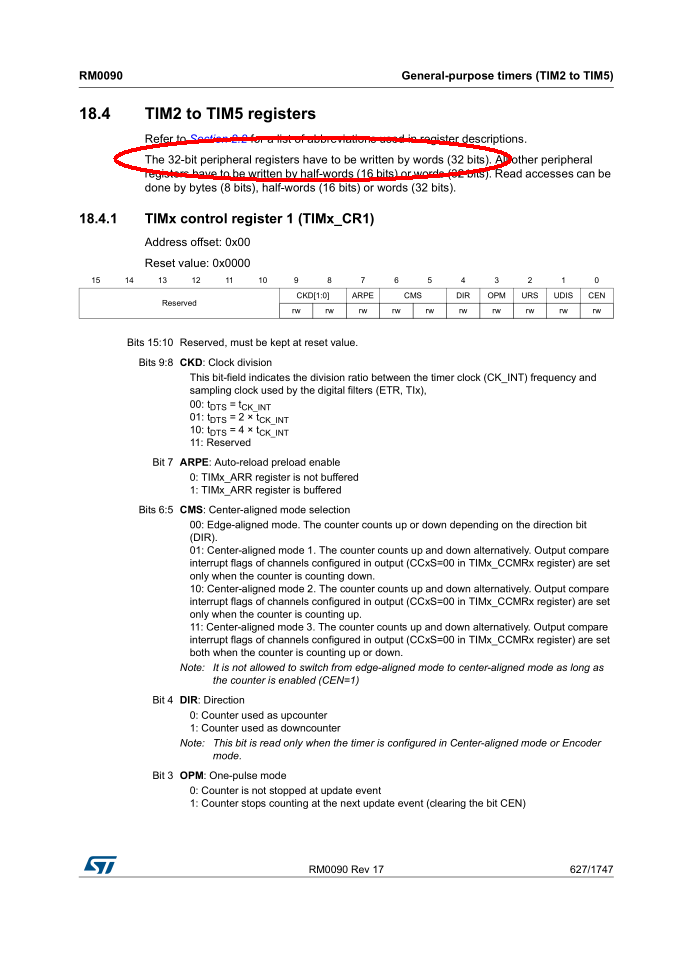
I think TIM2 on an F4 is going to want 32-bit writes.
Up vote any posts that you find helpful, it shows what's working..
- Mark as New
- Bookmark
- Subscribe
- Mute
- Subscribe to RSS Feed
- Permalink
- Email to a Friend
- Report Inappropriate Content
2018-10-11 3:49 AM
Yes that's it:
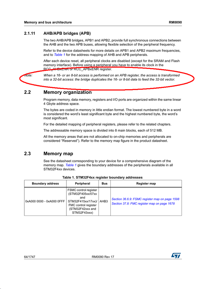
When the DMA writes 16-bits, the AHB-APB bridge doubles it.
There's no other rational solution than to have the values array 32-bit and tell the DMA to transfer words.
JW
- Mark as New
- Bookmark
- Subscribe
- Mute
- Subscribe to RSS Feed
- Permalink
- Email to a Friend
- Report Inappropriate Content
2018-10-11 4:16 AM
Hello Clive,
thanks for being a reliable source of help again.
I tried two solutions: change the array to uint32_t and PSIZE and MSIZE accordingly. This works but leads to twice as big an array for no use. The other solution is to use TIM3 which has a 16 bit ARR which also works good.
I remember having read something about registers that need 32bit access but I couldn't find out how to identify them in the ref manual. Please can you give some background information, also links for further reading are welcome.
Thanks a lot.
Martin
- Mark as New
- Bookmark
- Subscribe
- Mute
- Subscribe to RSS Feed
- Permalink
- Email to a Friend
- Report Inappropriate Content
2018-10-11 4:25 AM

Also, the DMA chapter's "packing/unpacking" table reveals, that in the 'F2/'F4/'F7 DMA there's no way to zero-pad data automatically; this is in contrast to the 'F1/'L1/'F0/'L0/'L4 DMA.
JW
- Mark as New
- Bookmark
- Subscribe
- Mute
- Subscribe to RSS Feed
- Permalink
- Email to a Friend
- Report Inappropriate Content
2018-10-11 5:57 AM
Hello Jan,
Thank you very much for your detailed answer and for pointing to the ref manual lines.
Can we make a general rule that this doubling of 16 bit accesses applies to any peripheral that has an enable bit in an RCC_APBx_ENR? Is it the case for all STM32 families, maybe even for all Cortex-Mx because it is subject to ARM IP ?
Thanks a lot
Martin
- Mark as New
- Bookmark
- Subscribe
- Mute
- Subscribe to RSS Feed
- Permalink
- Email to a Friend
- Report Inappropriate Content
2018-10-11 9:46 AM
> Can we make a general rule that this doubling of 16 bit accesses applies to any peripheral that has an enable bit in an RCC_APBx_ENR?
The "doubling" happens at the AHB-to-APB bridge, so if a master (processor or DMA -other masters, DMA-capable peripherals such as ETH and OTG_HS, generally don't support other than whole word-wide accesses) writes a byte or a halfword, the peripheral sees it on the APB's data bus doubled. But - and this is a big but - the lane (i.e. which bytes are used) information is also propagated from AHB to APB, so peripherals which are 16-bit or 8-bit access capable, will use this information and will use only the respective portion of the data. To sum it up, the width of access for given peripheral's registers, which is always given at the beginning of the register's subchapter, is always to be obeyed when writing to that peripheral, be it from processor or from DMA.
> Is it the case for all STM32 families
AFAIK, Yes. Read the respective RMs if you want to be sure.
Nonetheless, as I pointed out above, the DMA in some other STM32's works differently, so the net effect of the whole DMA-to-peripheral chain may be different in different families.
> maybe even for all Cortex-Mx because it is subject to ARM IP
No. I don't know where the AHB-to-APB bridge in STM32 originated, but I suspect it's ST's own. Even if it would be ARM's, other vendors may chose their own implementation.
JW
- Timer options for DMA transfer on STM32F03F4P6 in STM32 MCUs Products
- Overrun problem with USART2 in STM32H723 MCU in STM32 MCUs Embedded software
- STM32H7S3L8 LL DMA USART TX transfer in STM32 MCUs Products
- ADC in DMA circular mode with LL Library Problems in STM32 MCUs Embedded software
- STM32H7 U(S)ART Low Level RS485-DE Pin not switching in STM32 MCUs Products
