- STMicroelectronics Community
- STM32 MCUs
- STM32 MCUs Products
- STM32H730VBT6 SPI port mappable to OCTOSPI interfa...
- Subscribe to RSS Feed
- Mark Topic as New
- Mark Topic as Read
- Float this Topic for Current User
- Bookmark
- Subscribe
- Mute
- Printer Friendly Page
STM32H730VBT6 SPI port mappable to OCTOSPI interface?
- Mark as New
- Bookmark
- Subscribe
- Mute
- Subscribe to RSS Feed
- Permalink
- Email to a Friend
- Report Inappropriate Content
2024-03-26 11:12 PM
We have a custom board prototype with a STM32H730VBT6 (LQFP100 package) and a SPI NOR flash memory.
Sadly, this not connected to the OCTOSPIM_P1 port, but to the SPI1_NSS, SPI1_SCK, SPI1_MISO, SPI1_MISO (PA4, PA5, PA6, PB5) port (so, ony 2 data lines are connected, classic SPI).
Now, our application will not fit into internal flash (nor into RAM), so we are captive to use external memory for our program. How can we solve it, except make a new board? Some questions more in detail:
1. Can SPI1 be mapped somehow to OCTOSPI1?
2. Is it (physically or software-wise) possible at all to use that SPI1 connected chip as memory?
I'd probably would have to reprogram the whole memory protocol (command, address, alternate bytes and data phase...)?
3. What features are possible: DTR? Dual-line SPI? Memory-mapped mode?
(I think, at least the latter is impossible, if the answer to 1. is no.)
4. Is it possible to execute-in-place from that memory?
(I think not, if it cannot be brought into memory-mapped mode.)
Can You shed some light, and maybe also confirm or refute my assumptions?
Thank You very much!
- Labels:
-
OctoSPI
-
SPI
-
STM32H7 series
- Mark as New
- Bookmark
- Subscribe
- Mute
- Subscribe to RSS Feed
- Permalink
- Email to a Friend
- Report Inappropriate Content
2024-03-27 12:17 AM - edited 2024-03-27 12:18 AM
Have you already checked the datasheet for alternate functions on the used SPI1 pins?
- Mark as New
- Bookmark
- Subscribe
- Mute
- Subscribe to RSS Feed
- Permalink
- Email to a Friend
- Report Inappropriate Content
2024-03-27 1:18 AM - edited 2024-03-27 1:21 AM
Yes. But the only PIN that's shared with some OCTOSPI function is SPI_MISO, PA6, usable as OCTOSPIM_P1_IO3. But IO3 is not used on the memory chip anyway (connected to V+ there).
In the meantime I checked the options we have with a hardware change (welding manually) - there would be one. But this thread shall be completely about software- and register-wise solutions.
(To be able to compare the efforts.-)
- Mark as New
- Bookmark
- Subscribe
- Mute
- Subscribe to RSS Feed
- Permalink
- Email to a Friend
- Report Inappropriate Content
2024-03-27 10:58 PM
Can someone confirm or refute my assumption: No chance without hardware change to use that memory for the application code?
@LCEmaybe?
- Mark as New
- Bookmark
- Subscribe
- Mute
- Subscribe to RSS Feed
- Permalink
- Email to a Friend
- Report Inappropriate Content
2024-03-27 11:08 PM
Simple SPI flash (not QSPI/OSPI) does not work in memory mapped mode. Not possible to run XIP code from there.
But H730 has large RAM. Can you divide the code to overlays, store them in the flash and copy the parts into RAM to execute? Be creative.
- Mark as New
- Bookmark
- Subscribe
- Mute
- Subscribe to RSS Feed
- Permalink
- Email to a Friend
- Report Inappropriate Content
2024-03-27 11:51 PM
Pavel's idea seems to be the only way with current hardware.
These are the times one wishes it was an FPGA... ;)
- Mark as New
- Bookmark
- Subscribe
- Mute
- Subscribe to RSS Feed
- Permalink
- Email to a Friend
- Report Inappropriate Content
2024-03-28 12:55 AM
Thanks for Your Input!
The idea to execute codeparts from RAM I had too. That's the "BootROM support" of AN5188, in opposite to the "Execute in place (XiP) support", right?
> But H730 has large RAM.
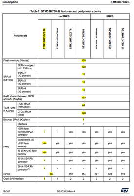
What "large" RAM do You mean? ;) This is the information I have from the Datasheet:
With this the code will probably not fit into memory, not even with all memory summed up - just an estimation. We plan several UART-based protocols, and several Ethernet-based protocols. Especially the latter I see producing quite a large code. Any opposite estimations?
So, I end up with quite some software-side effort to manage the memory and the shoveling? It's no blocker, but I must take that into conideration.
- Mark as New
- Bookmark
- Subscribe
- Mute
- Subscribe to RSS Feed
- Permalink
- Email to a Friend
- Report Inappropriate Content
2024-03-28 5:06 AM
Are you using lots of pictures ?
I'm using a large UART debug protocol file, have ethernet with lwip, http server, and current flash use is at 350 kB.
- Mark as New
- Bookmark
- Subscribe
- Mute
- Subscribe to RSS Feed
- Permalink
- Email to a Friend
- Report Inappropriate Content
2024-03-28 5:39 AM
I know, a display is planned too, I'm not sure about pictures on there.
I made a small test bringung up ethernet (from a rust example), and it went already above 128 KiB. That's where I took my assumption, that the whole thing will not fit. But thanks for the "counter estimation", that You got stuff running at 350 KiB. Still, also this already would take some efforts to get the code from the external flash into several RAM banks. (I haven't dealt with this yet.)
- Mark as New
- Bookmark
- Subscribe
- Mute
- Subscribe to RSS Feed
- Permalink
- Email to a Friend
- Report Inappropriate Content
2024-03-28 6:39 AM - edited 2024-03-28 6:40 AM
> What "large" RAM do You mean?
More than 128 KB ))
Rust.... :face_with_rolling_eyes:
