- STMicroelectronics Community
- STM32 MCUs
- STM32 MCUs Products
- STM32H725ZGT6 hangs after programming
- Subscribe to RSS Feed
- Mark Topic as New
- Mark Topic as Read
- Float this Topic for Current User
- Bookmark
- Subscribe
- Mute
- Printer Friendly Page
STM32H725ZGT6 hangs after programming
- Mark as New
- Bookmark
- Subscribe
- Mute
- Subscribe to RSS Feed
- Permalink
- Email to a Friend
- Report Inappropriate Content
2023-12-01 7:14 AM
Hello friends,
i have the following setup:
- STM32H725ZGT6 on a selfmade board.
- STM32 CubeMX (default program with HSI clock and without any other peripherals).
- Keil µVision 5.23
- ULINK2 Debugger
problem:
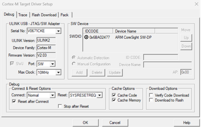
- I can program the controller ("verify successfull" by Keil) several times. The ULINK2 recognizes the controller (see IDCODE in the picture below)
- but as soon as i restart the power supply of the board (or press "debug" in Keil), the controller hangs and cannot be programmed again. In this state, the IDCODE is also not recognized anymore).
What could be the reason for this?
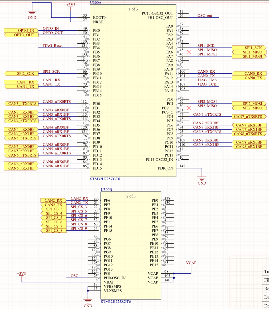
I have connected the signals:
- NRST (Pin27) to +3V3
- BOOT0 (Pin135) to GND
- PDR_ON (Pin142) to GND
- +3V3 on all VDDs, GND to all GNDs
- SWDIO (Pin102) to SWDIO (ULINK2)
- SWCLK (Pin107) to SWCLK (ULINK2)
- GND to GND (ULINK2)
- NJTRST (Pin131) to NRST(ULINK2)
I think the error must be somewhere in the hardware.
I tested the toolchain on a Nucleo Board (STM32H723ZGT6) and all works fine there.
I you need more information on this, please let me know.
Thanks for your help.
Regards, Tim
Solved! Go to Solution.
- Labels:
-
STM32H7 series
Accepted Solutions
- Mark as New
- Bookmark
- Subscribe
- Mute
- Subscribe to RSS Feed
- Permalink
- Email to a Friend
- Report Inappropriate Content
2023-12-04 5:56 AM
You might find the hardware design guide useful as it goes over these types of things:
Note that VCAP1 and VCAP2 each need a 2.2uF to ground. Will likely work okay with just one, but it's easy enough to follow the recommendations if you're building a new board.
Pullup on NRST is not needed, just a 0.1uF to GND. Won't hurt anything.
- Mark as New
- Bookmark
- Subscribe
- Mute
- Subscribe to RSS Feed
- Permalink
- Email to a Friend
- Report Inappropriate Content
2023-12-01 8:01 AM - edited 2023-12-01 8:16 AM
> NRST (Pin27) to +3V3
NRST should be bypassed to GND with a 0.1 uF capacitor. It should not be tied to 3.3V
(wrote the below before finding the above red flag)
If the code works on a nucleo board but not your custom board, the issue is likely the custom board and not your software configuration. Showing your schematic would be helpful, but here are the typical culprits:
- Are all VDD/VDDA pins tied to VCC?
- Area all VSS/VSSA pins tied to GND?
- Are VCAP bypassed only to GND with 2.2uF or 4.7uF?
Edit: PDR_ON should generally be tied to VCC unless you want to disable the regulator, which is uncommon.
- Mark as New
- Bookmark
- Subscribe
- Mute
- Subscribe to RSS Feed
- Permalink
- Email to a Friend
- Report Inappropriate Content
2023-12-01 9:07 AM
Check voltage on VCAP pins.
On the software side, as your code WILL RUN, double check HSE_VALUE define, LDO/SMPS settings, VOS settings, PLL settings in SystemClock_Config(). Make sure you're not violating the PLL / VCO limits.
Ideally you should be able to jumper BOOT0, you want it low for normal operation, but being able to pull it High and cycle power completely a couple of times will help to establish if it's YOUR CODE breaking things.
Up vote any posts that you find helpful, it shows what's working..
- Mark as New
- Bookmark
- Subscribe
- Mute
- Subscribe to RSS Feed
- Permalink
- Email to a Friend
- Report Inappropriate Content
2023-12-02 1:39 AM
Good morning,
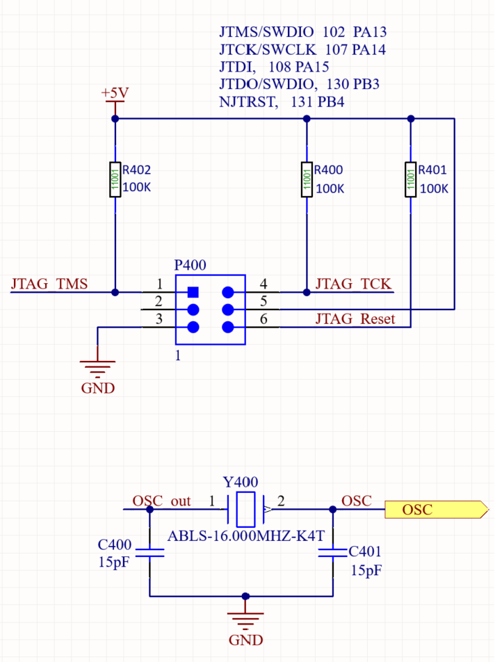
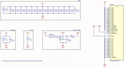
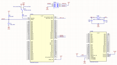
thank you for your quick replys and the suggestions. I have attached my controller schematics below.
i have tried the following adjustments:
- Removed the 3 pull ups R400-R402 (as 5V is wrong and the STM has internal Pull-ups, as i understand it).
- Added a 0,1µF from GND to +3V3 nearby the NRST.
- tied PDR_ON to +3V3
- added 2,2µF to VCAP
- connected BOOT0 to +3V3 instead of GND. But controller still hangs
- Mark as New
- Bookmark
- Subscribe
- Mute
- Subscribe to RSS Feed
- Permalink
- Email to a Friend
- Report Inappropriate Content
2023-12-02 2:08 AM - edited 2023-12-02 2:09 AM
I mean your schematics is complete wrong around SMPS and too STMLink isnt JTAG interface. Then JTAGRST is fail connected too.
Boot0 on GND was ok , but better is puldown 10k.
NRST (this connect to P400 rst) on 3V3 is fail, required is NC or pullup 10k to 3V3.
- Mark as New
- Bookmark
- Subscribe
- Mute
- Subscribe to RSS Feed
- Permalink
- Email to a Friend
- Report Inappropriate Content
2023-12-02 6:16 AM
> Added a 0,1µF from GND to +3V3 nearby the NRST.
Sonds like NRST is still tied to 3.3V. This is still a problem as it prevents the chip from being able to reset.
- Mark as New
- Bookmark
- Subscribe
- Mute
- Subscribe to RSS Feed
- Permalink
- Email to a Friend
- Report Inappropriate Content
2023-12-04 5:12 AM
Hello,
thank you very much for your answers.
I have made the following changes in the schematics by now:
- SWD signals: removed pull-up resistors
- BOOT0: 10kOhm to a switch (instead tied to GND).
- PDR_ON: tied to +3V3 (instead of GND)
- NRST: 10k pull-up, 100nF to GND, connected to RESET from ULINK. (instead of tied to GND)
- VLXSMPS floating (instead of tied to GND)
- VCAP: 2,2nF (instead of 3x 100nF)
- VREF: 47Ohm to VDDA (instead of floating)
- VDDUSB (33,50): tied to +3V3 as they are unused. (instead of floating)
This should work, right?
I will order a new PCB with this design, as the current one is to filigree to do these changes.
Thanks again!
- Mark as New
- Bookmark
- Subscribe
- Mute
- Subscribe to RSS Feed
- Permalink
- Email to a Friend
- Report Inappropriate Content
2023-12-04 5:56 AM
You might find the hardware design guide useful as it goes over these types of things:
Note that VCAP1 and VCAP2 each need a 2.2uF to ground. Will likely work okay with just one, but it's easy enough to follow the recommendations if you're building a new board.
Pullup on NRST is not needed, just a 0.1uF to GND. Won't hurt anything.
- Double buffer flicker / inequality in STM32 MCUs TouchGFX and GUI
- STM32C011J4M - issue with pin overlapp in STM32 MCUs Products
- Programming OSPI flash of STM32U5G-DK1 in Indirect memory mode in STM32 MCUs Products
- Cannot find/enable CMSIS-DSP (arm_math.h) on STM32N6570-DK via STM32CubeMX in STM32CubeMX (MCUs)
- STM32H563ZIT6 external loader fail in STM32 MCUs Embedded software
