- STMicroelectronics Community
- STM32 MCUs
- STM32 MCUs Products
- STM32F722 reads mostly incorrect values from SDRAM
- Subscribe to RSS Feed
- Mark Topic as New
- Mark Topic as Read
- Float this Topic for Current User
- Bookmark
- Subscribe
- Mute
- Printer Friendly Page
STM32F722 reads mostly incorrect values from SDRAM
- Mark as New
- Bookmark
- Subscribe
- Mute
- Subscribe to RSS Feed
- Permalink
- Email to a Friend
- Report Inappropriate Content
2018-07-03 3:05 AM
I'm using a custom board with F722 running at 160 MHz and a Micron 16 x 4 x 16 SDRAM presumably at 80 MHz. The following test program, however, yields wrong, but not entirely wrong values:
#define SDRAM_BASE ((uint32_t)0x60000000)
for (int i = 0; i < 256; ++i) *(__IO uint16_t*) (SDRAM_BASE + 2*i) = (i << 8) + i; for (int i = 0; i < 256; ++i) { int x = *(__IO uint16_t*) (SDRAM_BASE + 2*i); if (x != (i << 8) + i) printf('Index %x read %x != %x', i, x, (i << 8) + i); }The output for this is
Index 0 read 20 != 0
Index 1 read 21 != 101 Index 2 read 22 != 202 Index 3 read 23 != 303 ... Index f read 2f != f0f Index 10 read 30 != 1010 Index 11 read 31 != 1111 Index 12 read 32 != 1212 Index 13 read 33 != 1313 Index 14 read 34 != 1414 ... Index 1f read 3f != 1f1f Index 20 read 20 != 2020 Index 21 read 21 != 2121 Index 22 read 22 != 2222 Index 23 read 23 != 2323 Index 24 read 24 != 2424 ... Index 2f read 2f != 2f2f Index 30 read 30 != 3030 Index 31 read 31 != 3131 Index 32 read 32 != 3232 Index 33 read 33 != 3333 ...Some bit seems stuck, and the upper byte is missing completely. I also tried disabling byte access and set NBL[1:0], which is connected to DMQH/DMQL, to HIGH, but this didn't have any effect. The result is also stable, i.e. I can reproduce it by re-running the test.
If I enlarge the range and change my code from words to bytes,
for (int i = 0; i < 8192; ++i)
*(__IO uint8_t*) (SDRAM_BASE + i) = i % 256; // read bytes similarlythe test suddenly
succeeds
. But if I spread out the test to even addresses,for (int i = 0; i < 8192; ++i) {
*(__IO uint8_t*) (SDRAM_BASE +2*i
) = i % 256;I get errors again:
Index 0 read 20 != 0
Index 1 read 21 != 1 Index 2 read 22 != 2 Index 3 read 23 != 3 ... Index f read 2f != f Index 10 read 30 != 10 Index 11 read 31 != 11 Index 12 read 32 != 12 Index 13 read 33 != 13 ...I built two boards, and both behave the same. My configuration was generated by CubeMX:
hsdram1.Instance = FMC_SDRAM_DEVICE;
/* hsdram1.Init */ hsdram1.Init.SDBank = FMC_SDRAM_BANK1; hsdram1.Init.ColumnBitsNumber = FMC_SDRAM_COLUMN_BITS_NUM_9; hsdram1.Init.RowBitsNumber = FMC_SDRAM_ROW_BITS_NUM_13; hsdram1.Init.MemoryDataWidth = FMC_SDRAM_MEM_BUS_WIDTH_16; hsdram1.Init.InternalBankNumber = FMC_SDRAM_INTERN_BANKS_NUM_4; hsdram1.Init.CASLatency = FMC_SDRAM_CAS_LATENCY_2; hsdram1.Init.WriteProtection = FMC_SDRAM_WRITE_PROTECTION_DISABLE; hsdram1.Init.SDClockPeriod = FMC_SDRAM_CLOCK_PERIOD_2; hsdram1.Init.ReadBurst = FMC_SDRAM_RBURST_ENABLE; hsdram1.Init.ReadPipeDelay = FMC_SDRAM_RPIPE_DELAY_0; /* SdramTiming */ SdramTiming.LoadToActiveDelay = 2; SdramTiming.ExitSelfRefreshDelay = 6; SdramTiming.SelfRefreshTime = 3; SdramTiming.RowCycleDelay = 5; SdramTiming.WriteRecoveryTime = 2; SdramTiming.RPDelay = 2; SdramTiming.RCDDelay = 2;I added the SDRAM config sequence from the FMC example:
__IO uint32_t tmpmrd =0;
/* Step 3: Configure a clock configuration enable command */ Command.CommandMode = FMC_SDRAM_CMD_CLK_ENABLE; Command.CommandTarget = FMC_SDRAM_CMD_TARGET_BANK1; Command.AutoRefreshNumber = 1; Command.ModeRegisterDefinition = 0; HAL_SDRAM_SendCommand(&hsdram1, &Command, SDRAM_TIMEOUT); /* Step 4: Insert 100 us minimum delay */ HAL_Delay(1); /* Step 5: Configure a PALL (precharge all) command */ Command.CommandMode = FMC_SDRAM_CMD_PALL; Command.CommandTarget = FMC_SDRAM_CMD_TARGET_BANK1; Command.AutoRefreshNumber = 1; Command.ModeRegisterDefinition = 0; HAL_SDRAM_SendCommand(&hsdram1, &Command, SDRAM_TIMEOUT); /* Step 6 : Configure a Auto-Refresh command */ Command.CommandMode = FMC_SDRAM_CMD_AUTOREFRESH_MODE; Command.CommandTarget = FMC_SDRAM_CMD_TARGET_BANK1; Command.AutoRefreshNumber = 8; Command.ModeRegisterDefinition = 0; HAL_SDRAM_SendCommand(&hsdram1, &Command, SDRAM_TIMEOUT); /* Step 7: Program the external memory mode register */ tmpmrd = (uint32_t)SDRAM_MODEREG_BURST_LENGTH_1 | SDRAM_MODEREG_BURST_TYPE_SEQUENTIAL | SDRAM_MODEREG_CAS_LATENCY_2 | SDRAM_MODEREG_OPERATING_MODE_STANDARD | SDRAM_MODEREG_WRITEBURST_MODE_SINGLE; Command.CommandMode = FMC_SDRAM_CMD_LOAD_MODE; Command.CommandTarget = FMC_SDRAM_CMD_TARGET_BANK1; Command.AutoRefreshNumber = 1; Command.ModeRegisterDefinition = tmpmrd; HAL_SDRAM_SendCommand(&hsdram1, &Command, SDRAM_TIMEOUT); /* Step 8: Set the refresh rate counter: (64 ms / 8192 x Freq) - 20 */ hsdram1.Instance->SDRTR |= ((uint32_t)605); // 2HCLKI also triedlarger timings,and CL=3, but nothing helped.
My PCB has 4 layers, the SDRAM signals are separated intothree groups:
second layer: addresses, lengths 3-9 mm
third layer: data, lengths 2-1 mm
bottom layer: control, lengths 0-6
CLK length: 0 mm
Iwould suspect either some misconfiguration or bad signal tracing, but I just don't know how to examinemy problemany further than this.
#sdram #fmc Note: this post was migrated and contained many threaded conversations, some content may be missing.- Labels:
-
FMC-FSMC
- Mark as New
- Bookmark
- Subscribe
- Mute
- Subscribe to RSS Feed
- Permalink
- Email to a Friend
- Report Inappropriate Content
2018-07-03 3:45 AM
Make sure to do testing with caching disabled
Show schematic for SDRAM, and pin configuration code
More complex data patterns might better illustrate stuck-at faults, or shorts between bits.
Up vote any posts that you find helpful, it shows what's working..
- Mark as New
- Bookmark
- Subscribe
- Mute
- Subscribe to RSS Feed
- Permalink
- Email to a Friend
- Report Inappropriate Content
2018-07-03 5:27 AM
I'm assuming all the required trace length matching was done properly. One suggestion is to disable the read bursting. Another WAG would be to double everything in SdramTiming.
- Mark as New
- Bookmark
- Subscribe
- Mute
- Subscribe to RSS Feed
- Permalink
- Email to a Friend
- Report Inappropriate Content
2018-07-03 6:07 AM
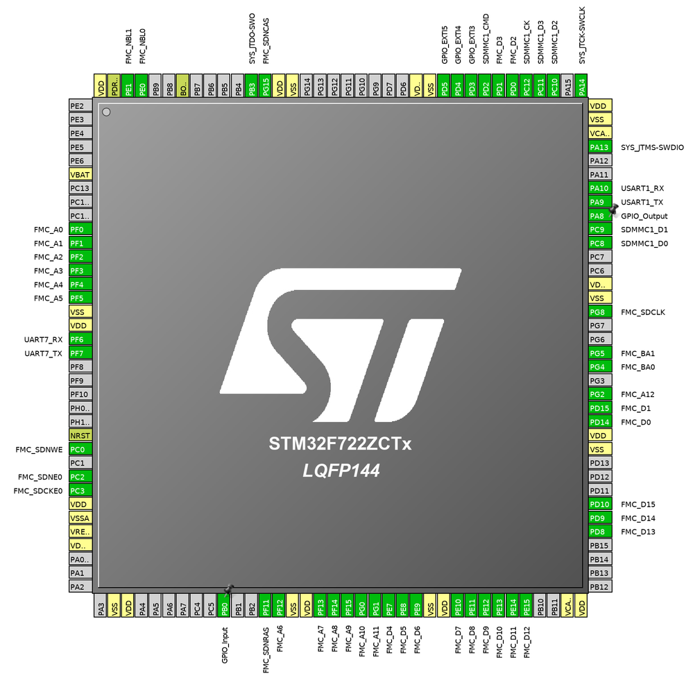
Here's the pin config code:
static void HAL_FMC_MspInit(void){
/* USER CODE BEGIN FMC_MspInit 0 */ /* USER CODE END FMC_MspInit 0 */ GPIO_InitTypeDef GPIO_InitStruct; if (FMC_Initialized) { return; } FMC_Initialized = 1; /* Peripheral clock enable */ __HAL_RCC_FMC_CLK_ENABLE(); /** FMC GPIO Configuration PF0 ------> FMC_A0 PF1 ------> FMC_A1 PF2 ------> FMC_A2 PF3 ------> FMC_A3 PF4 ------> FMC_A4 PF5 ------> FMC_A5 PC0 ------> FMC_SDNWE PC2 ------> FMC_SDNE0 PC3 ------> FMC_SDCKE0 PF11 ------> FMC_SDNRAS PF12 ------> FMC_A6 PF13 ------> FMC_A7 PF14 ------> FMC_A8 PF15 ------> FMC_A9 PG0 ------> FMC_A10 PG1 ------> FMC_A11 PE7 ------> FMC_D4 PE8 ------> FMC_D5 PE9 ------> FMC_D6 PE10 ------> FMC_D7 PE11 ------> FMC_D8 PE12 ------> FMC_D9 PE13 ------> FMC_D10 PE14 ------> FMC_D11 PE15 ------> FMC_D12 PD8 ------> FMC_D13 PD9 ------> FMC_D14 PD10 ------> FMC_D15 PD14 ------> FMC_D0 PD15 ------> FMC_D1 PG2 ------> FMC_A12 PG4 ------> FMC_BA0 PG5 ------> FMC_BA1 PG8 ------> FMC_SDCLK PD0 ------> FMC_D2 PD1 ------> FMC_D3 PG15 ------> FMC_SDNCAS PE0 ------> FMC_NBL0 PE1 ------> FMC_NBL1 */ /* GPIO_InitStruct */ GPIO_InitStruct.Pin = GPIO_PIN_0|GPIO_PIN_1|GPIO_PIN_2|GPIO_PIN_3 |GPIO_PIN_4|GPIO_PIN_5|GPIO_PIN_11|GPIO_PIN_12 |GPIO_PIN_13|GPIO_PIN_14|GPIO_PIN_15; GPIO_InitStruct.Mode = GPIO_MODE_AF_PP; GPIO_InitStruct.Pull = GPIO_NOPULL; GPIO_InitStruct.Speed = GPIO_SPEED_FREQ_VERY_HIGH; GPIO_InitStruct.Alternate = GPIO_AF12_FMC;HAL_GPIO_Init(GPIOF, &GPIO_InitStruct);/* GPIO_InitStruct */ GPIO_InitStruct.Pin = GPIO_PIN_0|GPIO_PIN_2|GPIO_PIN_3; GPIO_InitStruct.Mode = GPIO_MODE_AF_PP; GPIO_InitStruct.Pull = GPIO_NOPULL; GPIO_InitStruct.Speed = GPIO_SPEED_FREQ_VERY_HIGH; GPIO_InitStruct.Alternate = GPIO_AF12_FMC;HAL_GPIO_Init(GPIOC, &GPIO_InitStruct);/* GPIO_InitStruct */ GPIO_InitStruct.Pin = GPIO_PIN_0|GPIO_PIN_1|GPIO_PIN_2|GPIO_PIN_4 |GPIO_PIN_5|GPIO_PIN_8|GPIO_PIN_15; GPIO_InitStruct.Mode = GPIO_MODE_AF_PP; GPIO_InitStruct.Pull = GPIO_NOPULL; GPIO_InitStruct.Speed = GPIO_SPEED_FREQ_VERY_HIGH; GPIO_InitStruct.Alternate = GPIO_AF12_FMC; HAL_GPIO_Init(GPIOG, &GPIO_InitStruct); /* GPIO_InitStruct */ GPIO_InitStruct.Pin = GPIO_PIN_7|GPIO_PIN_8|GPIO_PIN_9|GPIO_PIN_10 |GPIO_PIN_11|GPIO_PIN_12|GPIO_PIN_13|GPIO_PIN_14 |GPIO_PIN_15|GPIO_PIN_0|GPIO_PIN_1; GPIO_InitStruct.Mode = GPIO_MODE_AF_PP; GPIO_InitStruct.Pull = GPIO_NOPULL; GPIO_InitStruct.Speed = GPIO_SPEED_FREQ_VERY_HIGH; GPIO_InitStruct.Alternate = GPIO_AF12_FMC; HAL_GPIO_Init(GPIOE, &GPIO_InitStruct); /* GPIO_InitStruct */ GPIO_InitStruct.Pin = GPIO_PIN_8|GPIO_PIN_9|GPIO_PIN_10|GPIO_PIN_14 |GPIO_PIN_15|GPIO_PIN_0|GPIO_PIN_1; GPIO_InitStruct.Mode = GPIO_MODE_AF_PP; GPIO_InitStruct.Pull = GPIO_NOPULL; GPIO_InitStruct.Speed = GPIO_SPEED_FREQ_VERY_HIGH; GPIO_InitStruct.Alternate = GPIO_AF12_FMC; HAL_GPIO_Init(GPIOD, &GPIO_InitStruct);}- Mark as New
- Bookmark
- Subscribe
- Mute
- Subscribe to RSS Feed
- Permalink
- Email to a Friend
- Report Inappropriate Content
2018-07-03 6:12 AM
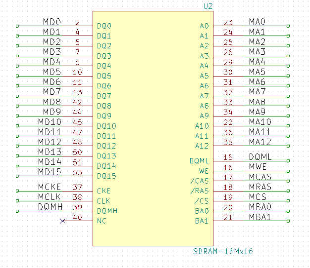
And here's my CubeMX config. All signals are connected to the obvious counterparts, and the non-obvious ones are SDNE0 -- CS, NBLE1/0 -- DQMH/L.

- Mark as New
- Bookmark
- Subscribe
- Mute
- Subscribe to RSS Feed
- Permalink
- Email to a Friend
- Report Inappropriate Content
2018-07-03 6:16 AM
I also noted something interesting. If I replace my data by a fixed constant 0x5555, i.e.,
for (int i = 0; i < 256; ++i)
*(__IO uint16_t*) (SDRAM_BASE + 2*i) = 0x5555;I still get this as result:
Index 0 read 20 != 5555
Index 1 read 21 != 5555 Index 2 read 22 != 5555 Index 3 read 23 != 5555 Index 4 read 24 != 5555 Index 5 read 25 != 5555 Index 6 read 26 != 5555 Index 7 read 27 != 5555 Index 8 read 28 != 5555 Index 9 read 29 != 5555 Index a read 2a != 5555 Index b read 2b != 5555 Index c read 2c != 5555 Index d read 2d != 5555 Index e read 2e != 5555 Index f read 2f != 5555 Index 10 read 30 != 5555 Index 11 read 31 != 5555 Index 12 read 32 != 5555 Index 13 read 33 != 5555It seems that I actually get parts of the address back -- how can that happen?
(Note: My pin assignment code seems to be waiting for moderator approval.)
- Mark as New
- Bookmark
- Subscribe
- Mute
- Subscribe to RSS Feed
- Permalink
- Email to a Friend
- Report Inappropriate Content
2018-07-03 6:17 AM
Two posts are waiting for moderation ...
- Mark as New
- Bookmark
- Subscribe
- Mute
- Subscribe to RSS Feed
- Permalink
- Email to a Friend
- Report Inappropriate Content
2018-07-03 6:19 AM
SDRAM schematic (9 column bits, 13 address bits):

- Mark as New
- Bookmark
- Subscribe
- Mute
- Subscribe to RSS Feed
- Permalink
- Email to a Friend
- Report Inappropriate Content
2018-07-03 11:38 AM
,
,
Ok, let me see if I can stand up some code independently
Which Micron Part ♯ specifically are you using, I want to pull the data-sheet?
Can I use USART1 PA9/PA10 for debug/diagnostic output?
Up vote any posts that you find helpful, it shows what's working..
- Mark as New
- Bookmark
- Subscribe
- Mute
- Subscribe to RSS Feed
- Permalink
- Email to a Friend
- Report Inappropriate Content
2018-07-03 12:24 PM
Yes, you can use USART1. The Micron SDRAM is part ♯ MT48LC16M16A2-7E.
Thank you so much!
- STM32G05 ADC problems adding IN8, IN9 or IN10 in STM32 MCUs Products
- Data corrupted when STM32G051 communicates to MicroSD in SPI mode in STM32 MCUs Embedded software
- STM32 Write to internal EEPROM only work once in STM32 MCUs Embedded software
- STSPIN32G4: No spin with encoder as main sensor in STM32 MCUs Motor control
- STM32F103VGT6 Channel 4 ADC acquisition pin malfunction in STM32 MCUs Products