- STMicroelectronics Community
- STM32 MCUs
- STM32 MCUs Products
- Re: ST-link v2 at 1.8V?
- Subscribe to RSS Feed
- Mark Topic as New
- Mark Topic as Read
- Float this Topic for Current User
- Bookmark
- Subscribe
- Mute
- Printer Friendly Page
ST-link v2 at 1.8V?
- Mark as New
- Bookmark
- Subscribe
- Mute
- Subscribe to RSS Feed
- Permalink
- Email to a Friend
- Report Inappropriate Content
2017-06-26 08:37 AM
I am using the ST-Link v2 with a target STM32 board running at 1.8V. I connect the 'target Vcc' to my boards Vcc ok, but the SWDIO and SWDCLK outputs from the ST-link are at 3.3V. Yet it looks like it is supposed to work down to 1.65V. How can I use it with my 1.8V board?
- Mark as New
- Bookmark
- Subscribe
- Mute
- Subscribe to RSS Feed
- Permalink
- Email to a Friend
- Report Inappropriate Content
2017-06-26 09:08 AM
The stand-alone ST-LINK provides a pin for the VTref (Target Voltage), this is used to power the IO buffers.
Is this an authentic ST-LINK, or a clone?
Perhaps you can diagram your circuit and connectivity.
Up vote any posts that you find helpful, it shows what's working..
- Mark as New
- Bookmark
- Subscribe
- Mute
- Subscribe to RSS Feed
- Permalink
- Email to a Friend
- Report Inappropriate Content
2017-06-26 09:50 AM
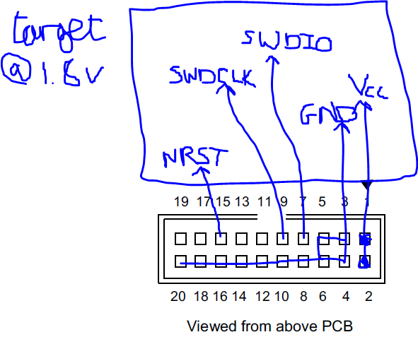
Apologies for crudity of diagram!
Yes it is a genuine brand new ST-link v2.
The target board has its own LiPo and regulator providing a Vcc of 1.8v. This is connected to pin 1 and 2 on the ST-Link as per the pinout diagram for SWD in UM1075.
If I just connect GND and Vcc then Vcc remains at 1.8v, but testing SWDIO and SWCLK they are both at 3.3v.
I expected the target voltage to vbe used to drive the other outputs as you say, but they don't seem to do that...?
- Mark as New
- Bookmark
- Subscribe
- Mute
- Subscribe to RSS Feed
- Permalink
- Email to a Friend
- Report Inappropriate Content
2017-06-26 10:28 AM
+1
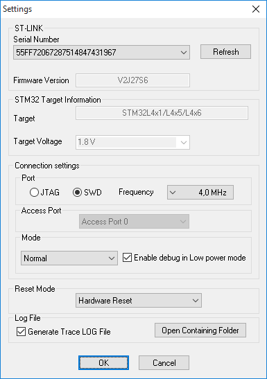
I see this exact same issue on my ST Link V2; paired with a STM32L4x6, using both STM32 ST-Link Utility and STM Workbench. Pin 1 Target VCC is steady 1.8V throughout, but the IO voltage on SW CLK and SWO are 3.3V. The voltage coming back from MCU is 1.8V, as expected.
I can talk to the target just fine, but concerned about Vih and incorrect sampling; and of course over driving pin IO
- Mark as New
- Bookmark
- Subscribe
- Mute
- Subscribe to RSS Feed
- Permalink
- Email to a Friend
- Report Inappropriate Content
2017-06-26 11:54 AM
Mine is from Farnell and has U2 in place and does not look like a clone either.
A simple stand-alone test I did was to put 1.8v between Vcc (pins 1&2) and GND (pins 3,4,5,6,8,10,12,14,16,18,20) and then have a look at SWDIO (pin 7) and SWCLK (pin 9). On my system both are at 3.3V. We really need a schematic or some good inside knowledge of what's going on.
- Mark as New
- Bookmark
- Subscribe
- Mute
- Subscribe to RSS Feed
- Permalink
- Email to a Friend
- Report Inappropriate Content
2017-06-26 12:29 PM
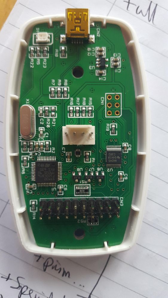
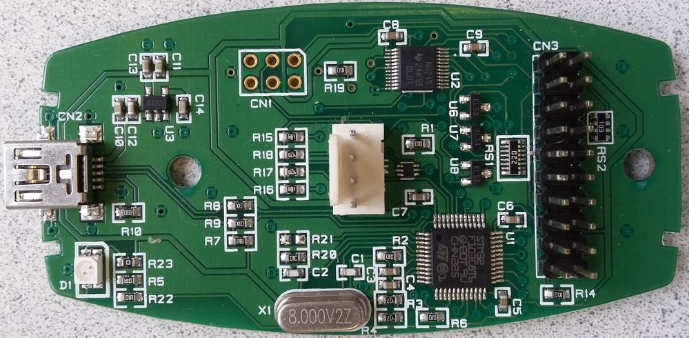
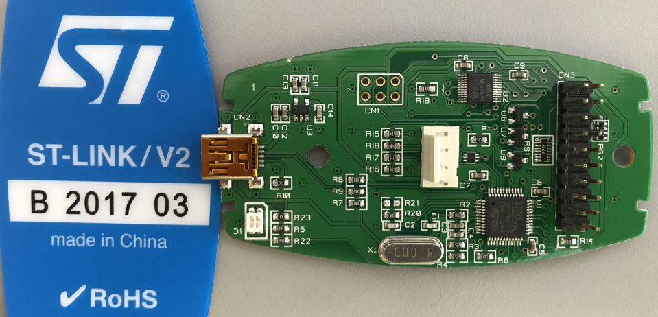
The clones don't have the level/buffer chip (245)
https://wiki.cuvoodoo.info/doku.php?id=jtag
This is what an official one looks like inside, U2 is the buffer chip
Up vote any posts that you find helpful, it shows what's working..
- Mark as New
- Bookmark
- Subscribe
- Mute
- Subscribe to RSS Feed
- Permalink
- Email to a Friend
- Report Inappropriate Content
2017-06-26 12:55 PM
Hi Clive, thanks for providing some insight.
For my adapter, purchased from Digikey, it looks like an authentic device per your U2 level shifter reference; same TI product package marking. Trace layout and the ground pours also look spot on, doesn't seem like a clone.
Any other thoughts?
- Mark as New
- Bookmark
- Subscribe
- Mute
- Subscribe to RSS Feed
- Permalink
- Email to a Friend
- Report Inappropriate Content
2017-06-26 01:05 PM
AS the SW pins are 5 V tolerant, it seems that the 3.3 V input to these pins is not dangerous. Also the ST-LINK main chip is STM32F103 with 3.3 V VCC, so the minimum VIH is 1.8 V. Therefore, the output of your chip will be correctly read by your ST-LINK.
- Mark as New
- Bookmark
- Subscribe
- Mute
- Subscribe to RSS Feed
- Permalink
- Email to a Friend
- Report Inappropriate Content
2017-06-26 01:30 PM
Thanks for your input, let's go two paths with this topic:
1) Why isn't STLink using 1.8V IO when target voltage is 1.8V?
I don't think this is answered. My understanding is 1.8V is a supported mode of operation (i.e. all IO voltages from STlink are 1.8V).
2) ST Link operating at 3.3V should be fine.
Looking at controller datasheet (STM32F103), Vih is the following.

If VDD is 3.3V + 5% (example accuracy tolerance of supply), then standard IO pin is 1.900V Vih. If SWO/CLK go to 5V tolerant pins on STLink, then 1.615V Vih. I didn't see an STLink schematic, so can't check the mapping. So depending on which pins this maps to, this might be more of a problem when talking with 1.8V target. The concern here is corner cases, especially with disparity caused by unexpected connector impedance or ground levels.
- Mark as New
- Bookmark
- Subscribe
- Mute
- Subscribe to RSS Feed
- Permalink
- Email to a Friend
- Report Inappropriate Content
2017-06-26 01:39 PM
I haven't been able to pin down a schematic to review.
Would recommend connecting 1.8V to pin 1 (VTREF) and Ground to pin 4 (GND), then without SWDIO/SWCLK connected, check the levels.
Up vote any posts that you find helpful, it shows what's working..
- STM32WL55jc1, how to boot the system without attaching the debugger (STLINK) in STM32CubeIDE (MCUs)
- Doubt in error rectification in STM32 MCUs Embedded software
- STM32Cube IDE problem flashing the code in STM32CubeIDE (MCUs)
- High power consumption in Stop mode with STLINKV3 connected in STM32 MCUs Products
- STM32CubeProgrammer v2.18.0 - missing DBANK/DUALBANK option bytes when cli is called in STM32CubeProgrammer (MCUs)
