- STMicroelectronics Community
- STM32 MCUs
- STM32 MCUs Products
- Re: serial data + clock + timer + dma 17 bit
- Subscribe to RSS Feed
- Mark Topic as New
- Mark Topic as Read
- Float this Topic for Current User
- Bookmark
- Subscribe
- Mute
- Printer Friendly Page
serial data + clock + timer + dma 17 bit
- Mark as New
- Bookmark
- Subscribe
- Mute
- Subscribe to RSS Feed
- Permalink
- Email to a Friend
- Report Inappropriate Content
2016-08-02 03:06 PM
Hello
need to implement such a protocol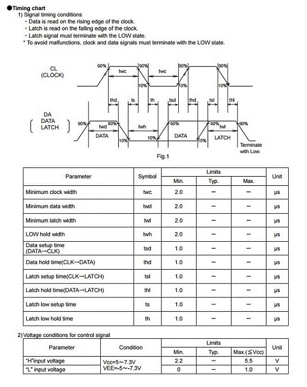
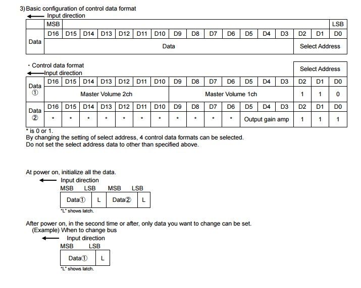 i need to make solution without interrupts and with DMA the main idea is send bufer with timer like here
 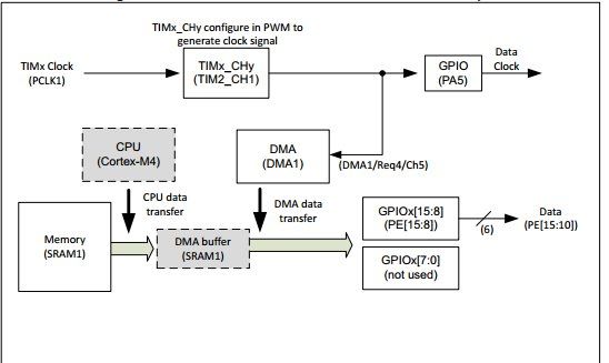 but cant conigure timer may be exist better idea than using timer or may be somebody can help to configure timer thx
- Mark as New
- Bookmark
- Subscribe
- Mute
- Subscribe to RSS Feed
- Permalink
- Email to a Friend
- Report Inappropriate Content
2016-08-02 07:06 PM
The fact it uses both clock phases, and that the data leads the clock means you need to drive the DMA with one timer channel, and then toggle another channel with delayed phase.
The alternative is to drive the clock as part of the GPIO DMA, at perhaps 4x the bit/clock rate, from a pattern buffer.Up vote any posts that you find helpful, it shows what's working..
- Mark as New
- Bookmark
- Subscribe
- Mute
- Subscribe to RSS Feed
- Permalink
- Email to a Friend
- Report Inappropriate Content
2016-08-03 03:19 AM
I would use a timer only to generate clocks - one channel in toggle mode for the clock to the device; other in PWM mode to generate a double-frequency clock, which I would then feed externally to SCK of a SPI, which in turn in slave mode would provide the data, feeding itself through DMA.
JW- Mark as New
- Bookmark
- Subscribe
- Mute
- Subscribe to RSS Feed
- Permalink
- Email to a Friend
- Report Inappropriate Content
2016-08-03 05:00 AM
need ''mask'' clock also - bcs need only 17 clocks for each bit transfer, and with latch no need clock , need drop down line
for example clock mask in bit ''101010101010101010101010101010101010''+''0''latchbitdata any 17 bit ''101010101010101010101010101010101010''+''1''latchbitand clock run after data- Mark as New
- Bookmark
- Subscribe
- Mute
- Subscribe to RSS Feed
- Permalink
- Email to a Friend
- Report Inappropriate Content
2016-08-03 05:08 AM
I did not understand your point.
You can try it in Russian if that's a language of your preference, I speak it a little bit.
JW- Mark as New
- Bookmark
- Subscribe
- Mute
- Subscribe to RSS Feed
- Permalink
- Email to a Friend
- Report Inappropriate Content
2016-08-03 06:42 AM
I'm reasonably sure that you will be able to do this using GPIO and DMA; I've used this approach in an STM32F405 to read a synchronous serial stream on both rising and falling edges. I didn't try to write to the stream, but I see no reason why it couldn't be done.
I should add that you CAN NOT use DMA1 to do this (on an F4 part, at least) because DMA1 cannot access the entire memory space; the GPIO registers are inaccessible to it. You can do it with DMA2 though because DMA2 can access the entire memory space; this means you have to use TIM1 or TIM8 because they're the only timers that can interact with DMA2.- Mark as New
- Bookmark
- Subscribe
- Mute
- Subscribe to RSS Feed
- Permalink
- Email to a Friend
- Report Inappropriate Content
2016-08-03 10:36 AM
cut task on two part:
1. Make Data signal/* TIM3 init function */
void MX_TIM3_Init(void)
{
TIM_MasterConfigTypeDef sMasterConfig;
TIM_OC_InitTypeDef sConfigOC;
htim3.Instance = TIM3;
htim3.Init.Prescaler = 0;
htim3.Init.CounterMode = TIM_COUNTERMODE_UP;
htim3.Init.Period = 168;
htim3.Init.ClockDivision = TIM_CLOCKDIVISION_DIV1;
HAL_TIM_PWM_Init(&htim3);
sMasterConfig.MasterOutputTrigger = TIM_TRGO_RESET;
sMasterConfig.MasterSlaveMode = TIM_MASTERSLAVEMODE_ENABLE;
HAL_TIMEx_MasterConfigSynchronization(&htim3, &sMasterConfig);
sConfigOC.OCMode = TIM_OCMODE_PWM1;
sConfigOC.Pulse = 0;
sConfigOC.OCPolarity = TIM_OCPOLARITY_HIGH;
sConfigOC.OCFastMode = TIM_OCFAST_DISABLE;
HAL_TIM_PWM_ConfigChannel(&htim3, &sConfigOC, TIM_CHANNEL_3);
HAL_TIM_MspPostInit(&htim3);
}void HAL_TIM_PWM_MspInit(TIM_HandleTypeDef* htim_pwm)
{
if(htim_pwm->Instance==TIM3)
{
/* USER CODE BEGIN TIM3_MspInit 0 */
/* USER CODE END TIM3_MspInit 0 */
/* Peripheral clock enable */
__HAL_RCC_TIM3_CLK_ENABLE();
/* Peripheral DMA init*/
hdma_tim3_ch3.Instance = DMA1_Stream7;
hdma_tim3_ch3.Init.Channel = DMA_CHANNEL_5;
hdma_tim3_ch3.Init.Direction = DMA_MEMORY_TO_PERIPH;
hdma_tim3_ch3.Init.PeriphInc = DMA_PINC_DISABLE;
hdma_tim3_ch3.Init.MemInc = DMA_MINC_ENABLE;
hdma_tim3_ch3.Init.PeriphDataAlignment = DMA_PDATAALIGN_WORD;
hdma_tim3_ch3.Init.MemDataAlignment = DMA_MDATAALIGN_WORD;
hdma_tim3_ch3.Init.Mode = DMA_NORMAL;
hdma_tim3_ch3.Init.Priority = DMA_PRIORITY_VERY_HIGH;
hdma_tim3_ch3.Init.FIFOMode = DMA_FIFOMODE_DISABLE;
HAL_DMA_Init(&hdma_tim3_ch3);
__HAL_LINKDMA(htim_pwm,hdma[TIM_DMA_ID_CC3],hdma_tim3_ch3);
/* USER CODE BEGIN TIM3_MspInit 1 */
/* USER CODE END TIM3_MspInit 1 */
}
}uint32_t buf[4] = {84, 84, 84, 0};
HAL_TIM_PWM_Start_DMA(&htim3, TIM_CHANNEL_3, buf, 4);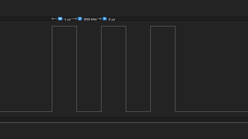 seems like ok, but i need 100% filling
uint32_t buf[4] = {168, 84, 84, 0};
HAL_TIM_PWM_Start_DMA(&htim3, TIM_CHANNEL_3, buf, 4);
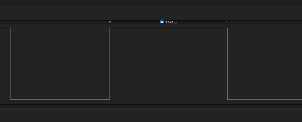 try to decreese value
uint32_t buf[4] = {162, 84, 84, 0};
HAL_TIM_PWM_Start_DMA(&htim3, TIM_CHANNEL_3, buf, 4);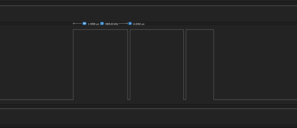 but its also fake
do :
uint32_t buf[4] = {161, 84, 84, 0};
HAL_TIM_PWM_Start_DMA(&htim3, TIM_CHANNEL_3, buf, 4);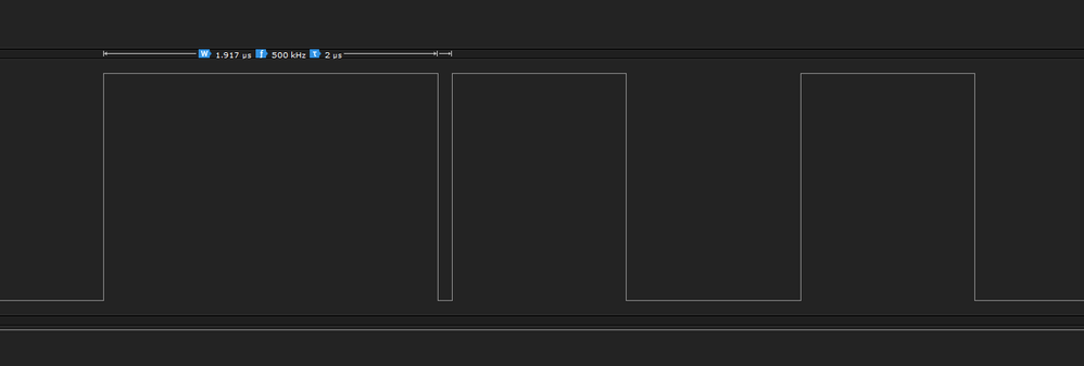 its looks like OK but its not 100% filled PWM
How to get 100% PWM in timer DMA mode?
Thx
- Mark as New
- Bookmark
- Subscribe
- Mute
- Subscribe to RSS Feed
- Permalink
- Email to a Friend
- Report Inappropriate Content
2016-08-04 04:04 AM
I don't use HAL so can't help you with the code, but I would trigger DMA from the update rather than from the CC channel, and make sure preload is enabled for the given CC register.
JW- Mark as New
- Bookmark
- Subscribe
- Mute
- Subscribe to RSS Feed
- Permalink
- Email to a Friend
- Report Inappropriate Content
2016-08-04 04:23 PM
If i run timer in
Output Compare -> mode Toggle on match
uint32_t clk[34] = {167, 0, 167, 0, 167, 0, 167, 0, 167, 0,
167, 0, 167, 0, 167, 0, 167, 0, 167, 0,
167, 0, 167, 0, 167, 0, 167, 0, 167, 0,
167, 0, 167, 169};
HAL_TIM_OC_Start_DMA(&htim3, TIM_CHANNEL_3, clk, 34); If i run timer in PWM mode
uint32_t data[35] = { 161, 0, 161, 0, 161, 0, 161, 0, 161, 0,
161, 0, 161, 0, 161, 0, 161, 0, 161, 0,
161, 0, 161, 0, 161, 0, 161, 0, 161, 0,
161, 0, 161, 161, 0};
HAL_TIM_PWM_Start_DMA(&htim3, TIM_CHANNEL_4, data, 35);
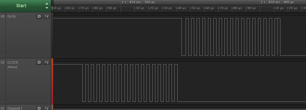 But in PWM mode i can make two HIGH impulses - its OK for DATA
Also i try to redirect DMA to
(GPIOC->BSRR) but no luck - always get
HAL_DMA_STATE_ERROR.:
uint32_t Length = 34;
htim3.State = HAL_TIM_STATE_BUSY;
htim3.hdma[TIM_DMA_ID_CC3]->XferCpltCallback = TIM_DMADelayPulseCplt;
htim3.hdma[TIM_DMA_ID_CC3]->XferErrorCallback = TIM_DMAError ;
HAL_DMA_Start_IT(htim3.hdma[TIM_DMA_ID_CC3], (uint32_t)pData1, (uint32_t)&(GPIOC->BSRR), Length);
__HAL_TIM_ENABLE_DMA(&htim3, TIM_DMA_CC3);
TIM_CCxChannelCmd(htim3.Instance, TIM_CHANNEL_3, TIM_CCx_ENABLE);
if(IS_TIM_ADVANCED_INSTANCE(htim3.Instance) != RESET)
{
__HAL_TIM_MOE_ENABLE(&htim3);
}
__HAL_TIM_ENABLE(&htim3);- Mark as New
- Bookmark
- Subscribe
- Mute
- Subscribe to RSS Feed
- Permalink
- Email to a Friend
- Report Inappropriate Content
2016-08-05 03:13 PM
Use a timer with multiple OC channels - you must use TIM1 or TIM8 anyway, because of the DMA issue that I've already mentioned. Do not try to use the timer to directly drive the clock signal.
e.g. If TIM1 is clocked at 100MHz, and you want to work at the maximum bus frequency of 250kHz, set PSC = 0, ARR = 400, CCR1 = 100, CCR2 = 200, CCR3 = 300. For each transmission, construct an array of data and latch bits. The last latch bit must be '0' and I presume that the others must be all '1'. Data: 0b10101010101011 Latch: 0b11111111111110 Configure the TIM and DMA to: Write your data pin to the next data bit value on TIMx update trigger. Write your clock pin to '1' on TIMx->CH1 trigger. Write your data pin to the next latch bit value on TIMx->CH2 trigger Write your clock pin to '0' on TIMx->CH3 trigger Use bitbanding to target the DMA transfers at particular bits in the data and latch arrays, and the GPIO ports.- Problem with DAC+DMA End-of-Transmission Interrupts on STM32L452RET6P in STM32 MCUs Products
- PWM no signal on TIM2 Channel1 and TIM3 Channel 1 in STM32 MCUs Products
- STM32H750 assembly: same delay loops, but one takes 5x longer? in STM32 MCUs Embedded software
- Greenhouse Temperature Controller - STM32H750BDK in STM32 MCUs Products
- How to implement PLL in STM32? in STM32 MCUs Motor control