- STMicroelectronics Community
- STM32 MCUs
- STM32 MCUs Products
- HELP !! FMC what is going on
- Subscribe to RSS Feed
- Mark Topic as New
- Mark Topic as Read
- Float this Topic for Current User
- Bookmark
- Subscribe
- Mute
- Printer Friendly Page
HELP !! FMC what is going on
- Mark as New
- Bookmark
- Subscribe
- Mute
- Subscribe to RSS Feed
- Permalink
- Email to a Friend
- Report Inappropriate Content
2019-11-09 10:46 AM
Hello
any help appreciated
trying to work out out how the FMC peripheral works on the STM32F767ZI arm
would like to interface an FPGA to the 767 arm as an external memory device using a multiplexed Address & Data Bus, but so little info on the FMC out there ???
I have hooked up all the hardware wiring between the FPGA and ARM and guess what, as usual really really strange thing happening ?
why when I use
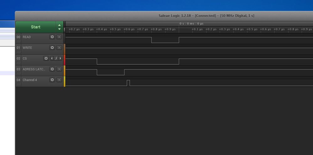
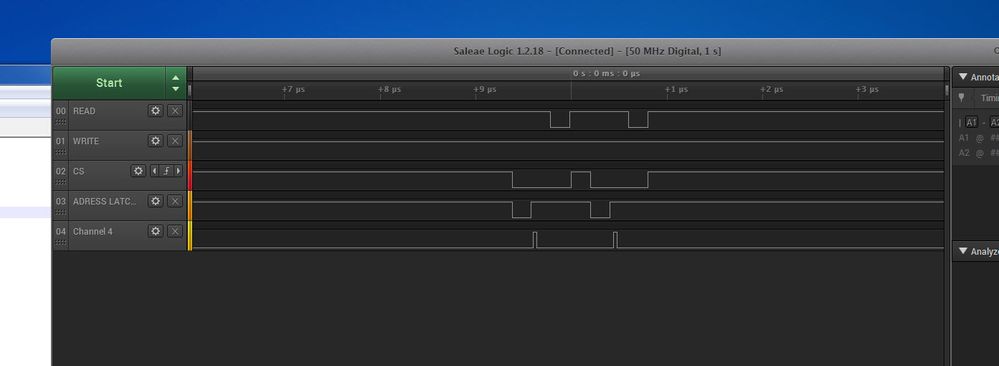
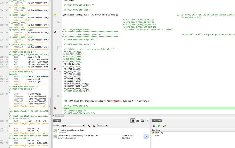
HAL_SRAM_Read_16b(&hsram1, (uint32_t *)0x60000001, (uint16_t *)rxBuffer, 1);
I get two chip selects and two reads
Yet when I read 60000000 I only get one CS and one read, WHAT IS GOING ON ???
HAL_SRAM_Read_16b(&hsram1, (uint32_t *)0x60000000, (uint16_t *)rxBuffer, 1);
Both these above HAL_SRAM_Read commands should simply read back ONE 16bit (2byte) data from the selected address
but anything above 0x60000000 does 2 chip selects and two reads of the data
is this a floored faulty FMC module
0x60000000 should = 1st 16bit address read
and
0x60000001 should - 2nd 16 bit address read (why 2 chip selects and 2 reads of data ??)
any help appreciated
Thank You
- Labels:
-
FMC-FSMC
-
STM32F7 series
- Mark as New
- Bookmark
- Subscribe
- Mute
- Subscribe to RSS Feed
- Permalink
- Email to a Friend
- Report Inappropriate Content
2019-11-09 11:24 AM
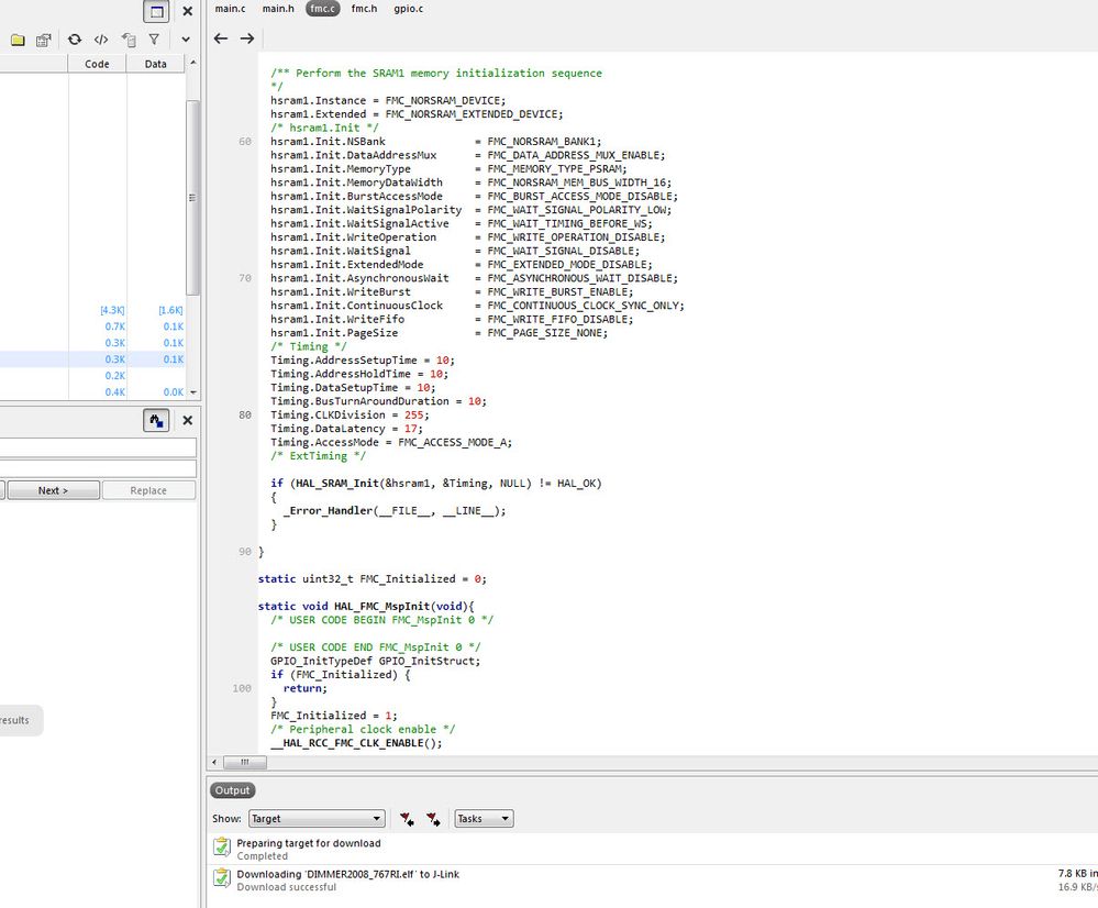
How wide is the DATA BUS?
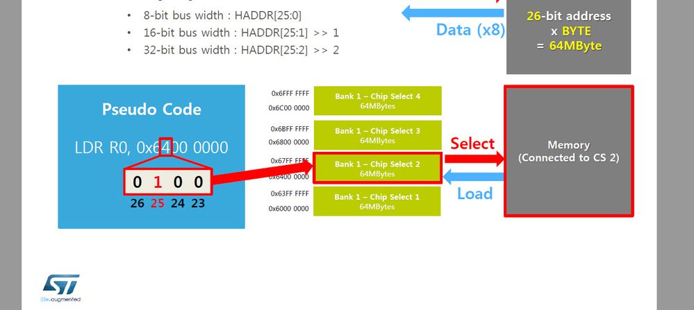
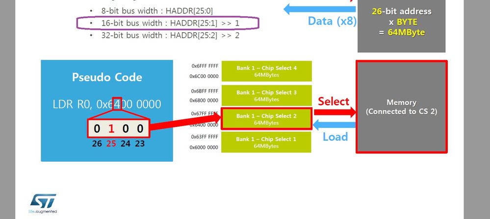
At 16-bit the memory address to the DEVICE changes from 0x60000000 to 0x60000002
If you read a 16-bit word at an ODD boundary it spans TWO words in the DEVICE
Up vote any posts that you find helpful, it shows what's working..
- Mark as New
- Bookmark
- Subscribe
- Mute
- Subscribe to RSS Feed
- Permalink
- Email to a Friend
- Report Inappropriate Content
2019-11-09 11:47 AM
hello
thank you for your reply
my data bus is 16 bits wide, i'm only interested in 16 bits address so address (16:23) not intrested
so I have 16 multiplexed address and data lines which should hopefully send out the 16bit address first over the 16 lines to the FPGA and then either write or read 16bits of data from or to the FPGA
so am I correct in thinking
0x60000000 = address 0 inside my FPGA
and 0x60000001 = address 1 inside my FPGA
and 0x60000002 = address 2 inside my FPGA
sorry I don't really understand ???
How wide is the DATA BUS? 16bits
At 16-bit the memory address to the DEVICE changes from 0x60000000 to 0x60000002
If you read a 16-bit word at an ODD boundary it spans TWO words in the DEVICE
How can I get over this ???
I simply would like to read or write only 16bits, not two lots of 8bits
Just a simple 16bit read or write of data
Thanks for any help
would I be better using a different CS memory address area for 16bit read and write say CS3 0x6800000 ???
sorry really confused are you saying it reads two lots of 8bit data consecutively thus the two cs lows ??
is there no way just to simply read and write 16bits of data
thanks
- Mark as New
- Bookmark
- Subscribe
- Mute
- Subscribe to RSS Feed
- Permalink
- Email to a Friend
- Report Inappropriate Content
2019-11-09 12:42 PM
>>so am I correct in thinking
0x60000000 = address 0 inside my FPGA
and 0x60000001 = address 1 inside my FPGA
and 0x60000002 = address 2 inside my FPGA
NO
With a 16-bit DATA BUS the DEVICE addresses as WORDS
0x60000000 = address 0 externally
and 0x60000002 = address 1
and 0x60000004 = address 2
>>sorry really confused are you saying it reads two lots of 8bit data consecutively thus the two cs lows ??
EVEN WORDs will go to your device directly
ODD ADDRESSED WORDs will span TWO WORDs in your DEVICE
0x60000001 will pull HALF of WORD 0, and HALF of WORD 1
BYTEs are manage via BYTE LANES. A Barrel shifter on the input to extract a 8-bit byte from the word, and a LOW/HIGH Byte Lane select for writes to a single byte within the word.
Up vote any posts that you find helpful, it shows what's working..
- Mark as New
- Bookmark
- Subscribe
- Mute
- Subscribe to RSS Feed
- Permalink
- Email to a Friend
- Report Inappropriate Content
2019-11-09 12:45 PM
ST Shifts the Internal Address Space to the External Bus, at 16-bit, ie IntA1 -> ExtA0
Up vote any posts that you find helpful, it shows what's working..
- Mark as New
- Bookmark
- Subscribe
- Mute
- Subscribe to RSS Feed
- Permalink
- Email to a Friend
- Report Inappropriate Content
2019-11-09 1:11 PM
thank you very much for your detailed info
so if i'm understanding you correctly
for me to read or write 16bits of data to the FPGA with a single chip correctly , I simply need to issue even address, 0x6000000, 0x60000002, 0x60000004 etc
if I issue odd address, I read or write half the data from one address and half from the next address ???
is this correct
really appreciate your help, as this has really confused me for the past day or so
Regards
- Mark as New
- Bookmark
- Subscribe
- Mute
- Subscribe to RSS Feed
- Permalink
- Email to a Friend
- Report Inappropriate Content
2019-11-09 1:23 PM
YES
The processor has byte addressability, you're attaching a word addressable device, there is a translation
For uint16_t *p = ( uint16_t *)0x60000000;
*p++ = 0x1234; // Writes to DEVICE ADDR 0
*p++ = 0x5678; // Writes to DEVICE ADDR 1 (advances pointer by 2)
Up vote any posts that you find helpful, it shows what's working..
- Mark as New
- Bookmark
- Subscribe
- Mute
- Subscribe to RSS Feed
- Permalink
- Email to a Friend
- Report Inappropriate Content
2019-11-09 1:27 PM
Thank you so much :)
- Mark as New
- Bookmark
- Subscribe
- Mute
- Subscribe to RSS Feed
- Permalink
- Email to a Friend
- Report Inappropriate Content
2019-11-09 1:54 PM
Hello again
so I guess I can not easily read consecutive data in a buffer array say 8bytes starting at 0x60000000
HAL_SRAM_Read_16b(&hsram1, (uint32_t *)0x60000000, (uint16_t *)rxBuffer, 8 );
or can I just ignore the odd data bytes in the array :)
Regards
- Mark as New
- Bookmark
- Subscribe
- Mute
- Subscribe to RSS Feed
- Permalink
- Email to a Friend
- Report Inappropriate Content
2019-11-10 10:05 PM
If your chip can handle unaligned data (I guess most STM32s can), you can read 16-bit data from an odd address. The HW just splits the access into 2 byte accesses, but the value should be right in the destination register. You can also read array of half words starting from zero, or array of bytes starting from zero. What's the problem here?
- Double buffer flicker / inequality in STM32 MCUs TouchGFX and GUI
- Questions regarding STM32U5 Flash endurance in STM32 MCUs Products
- Cannot find/enable CMSIS-DSP (arm_math.h) on STM32N6570-DK via STM32CubeMX in STM32CubeMX (MCUs)
- Going back to older version of code in Others: STM32 MCUs related
- STLINK-V3PWR to Nucleo board SWD in STM32 MCUs Boards and hardware tools
