Turn on suggestions
Auto-suggest helps you quickly narrow down your search results by suggesting possible matches as you type.
Showing results for
- STMicroelectronics Community
- STM32 MCUs
- STM32 MCUs Products
- F429 + SDRAM PCB Design
Options
- Subscribe to RSS Feed
- Mark Topic as New
- Mark Topic as Read
- Float this Topic for Current User
- Bookmark
- Subscribe
- Mute
- Printer Friendly Page
F429 + SDRAM PCB Design
Options
- Mark as New
- Bookmark
- Subscribe
- Mute
- Subscribe to RSS Feed
- Permalink
- Email to a Friend
- Report Inappropriate Content
2014-09-27 10:57 AM
Posted on September 27, 2014 at 19:57
Hello,
i am currently working on my first PCB with a STM32. The F429 and the SDRAM have LQFP/TSOP packages. Unfortunately the FMC Pins needed for SDRAM are distributed over all sides of the LQFP. I have looked on the gerber files of the F429 DISCO Board and not seen any measures to get all (data/address) lines to the same length. Well, the F429 can clock the SDRAM at max. of 90 MHz. How critical are different wire lengths under such conditions? Is there a (non religious!, just practical) design guide?
This discussion is locked. Please start a new topic to ask your question.
2 REPLIES 2
Options
- Mark as New
- Bookmark
- Subscribe
- Mute
- Subscribe to RSS Feed
- Permalink
- Email to a Friend
- Report Inappropriate Content
2014-09-28 12:19 AM
Posted on September 28, 2014 at 09:19
just keep it short. ideally put sdram below stm32f429.
Note that if you are going to use it in software access (not dma) it will run only to 22MTps (while sram will do 36MTps) so at this speed, any pcb will workOptions
- Mark as New
- Bookmark
- Subscribe
- Mute
- Subscribe to RSS Feed
- Permalink
- Email to a Friend
- Report Inappropriate Content
2014-09-28 3:13 PM
Posted on September 29, 2014 at 00:13
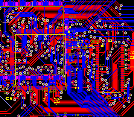
I have attached a pic of my solution to the problem and as you can see I haven?t managed to get the track lengths even either and I haven?t had any problems yet.
Putting it underneath would be a good idea but in my case that space is filled by a FPGA.
Related Content
- Can SDRAM Work with Cross-Connected FMC Lines on STM32H7? in STM32 MCUs Products
- TouchGFX LTDC Framebuffer Address for 800x600 Display with External eMMC (IS21ES08GA-JQLI) in STM32 MCUs TouchGFX and GUI
- Power consumption of STM32H5 MCU for VIO Pins in STM32 MCUs Products
- Why is FMC-SDRAM no longer supported on STM32H533 compared to STM32F446? in STM32 MCUs Products
- custom surveillance drone with STM32N657X0H3Q in STM32 MCUs Products