- STMicroelectronics Community
- STM32 MCUs
- STM32 MCUs Products
- Re: Data is not stored in the FIFO when FSEL is 1
- Subscribe to RSS Feed
- Mark Topic as New
- Mark Topic as Read
- Float this Topic for Current User
- Bookmark
- Subscribe
- Mute
- Printer Friendly Page
Data is not stored in the FIFO when FSEL is 1
- Mark as New
- Bookmark
- Subscribe
- Mute
- Subscribe to RSS Feed
- Permalink
- Email to a Friend
- Report Inappropriate Content
2024-02-20 9:19 AM
What I want to do is send Write Enable instruction to external Flash and erase.
The environment is as follows.
Use Board : nucleo l4r5zi
IDE : Atollic TrueSTUDIO® for STM32, Built on Eclipse Neon.1a.(Version: 9.3.0)
FLASH : W25Q64JV
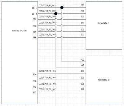
The connection diagram of the board and FLASH is shown below.
I want to send Write Enable instruction to 「W25Q64JV 2」.
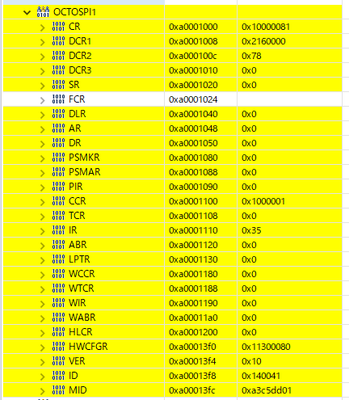
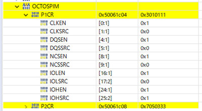
The registers are set as follows.
●OCTOSPI
●OCTOSPIM
I send Write Enable instruction and then the Read Status instruction. 0 is always stored in the FIFO. (Of course I make sure the FTF is set before reading the data register)
I assume that the setting on the microcontroller side is wrong because when I check IO5 with an oscilloscope, I get the expected waveform.
For your information, when I set FSEL to 0 and communicated with 「W25Q64JV 1」 using IO0~IO3, the data was stored in the FIFO as expected.
If there are any settings that are missing, I would like to know.
Solved! Go to Solution.
- Labels:
-
OctoSPI
-
STM32L4 Series
Accepted Solutions
- Mark as New
- Bookmark
- Subscribe
- Mute
- Subscribe to RSS Feed
- Permalink
- Email to a Friend
- Report Inappropriate Content
2024-02-23 6:06 AM
Hello,
I changed the IO5 pin from PC2 to PG11 and now the data is stored in the FIFO as expected.
The problem has been solved and is closed.
- Mark as New
- Bookmark
- Subscribe
- Mute
- Subscribe to RSS Feed
- Permalink
- Email to a Friend
- Report Inappropriate Content
2024-02-23 6:06 AM
Hello,
I changed the IO5 pin from PC2 to PG11 and now the data is stored in the FIFO as expected.
The problem has been solved and is closed.
- STM32 CubeIDE assembly code + C issue in STM32 MCUs Embedded software
- force input buffer for CRC to be aligned 32 bits in STM32 MCUs Embedded software
- getPixelData() Hardfault in STM32 MCUs TouchGFX and GUI
- Fail to load images from the SD card in STM32 MCUs TouchGFX and GUI
- Using Internal Flash as Eprom at External Flash Application in STM32 MCUs Embedded software


