- STMicroelectronics Community
- STM32 MCUs
- STM32 MCUs Products
- Re: Creating a raising edge to wake up the micro c...
- Subscribe to RSS Feed
- Mark Topic as New
- Mark Topic as Read
- Float this Topic for Current User
- Bookmark
- Subscribe
- Mute
- Printer Friendly Page
Creating a raising edge to wake up the micro controller
- Mark as New
- Bookmark
- Subscribe
- Mute
- Subscribe to RSS Feed
- Permalink
- Email to a Friend
- Report Inappropriate Content
2014-11-20 9:41 PM
Need help in understanding the
used by the STM32VLDISCOVERYboard.

The
http://www.st.com/st-web-ui/static/active/en/resource/technical/document/datasheet/CD00161566.pdf
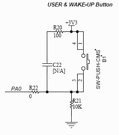
says the STM32 micro controller can be woken up by a raising edge. My interpretation is that the pull up resistor connected between the 3.3V and the wakeup pin will pull the wakeup pin high on power on. But I am not able to understand the use of the second resistor between the wake up pin and the ground. Will the two resistors not form a voltage divider circuit ? #stmvldiscovery- Mark as New
- Bookmark
- Subscribe
- Mute
- Subscribe to RSS Feed
- Permalink
- Email to a Friend
- Report Inappropriate Content
2014-11-21 12:56 AM
There are two microcontrollers in the design!
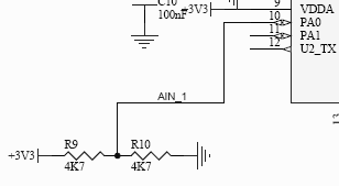
Reviewing the STM32VLDISCOVERY schematics (MB913.pdf), R9 and R10 provide an analogue signal to AIN1 on the STM32F103C8T6 (U2 ST LINK). The User Wakeup is shown as connecting to PA0 on U3A the STM32F100RBT6B (although R22 0R looks like it is intended to isolate the circuit).
- Mark as New
- Bookmark
- Subscribe
- Mute
- Subscribe to RSS Feed
- Permalink
- Email to a Friend
- Report Inappropriate Content
2014-11-21 10:56 AM
Thank you for explaining. However it will be helpful if you can explain the function of R1 and R2 in providing analog signal to the AIN1 on the STM32F103C8T6. As I understand R1 and R2 form a voltage divider circuit and pull down the voltage from 3.3V to 1.6V... However I am not able to understand the real intent of the resistors and the circuit they form.
- Mark as New
- Bookmark
- Subscribe
- Mute
- Subscribe to RSS Feed
- Permalink
- Email to a Friend
- Report Inappropriate Content
2014-11-24 6:25 AM
I imagine it is just to let the ST Link microcontroller monitor the +3V3 supply voltage. The signal is marked as AIN_1 so it's going to be input to the microcontroller's internal A to D converter ADC1. The potential divider just reduces the voltage from +3V3 to about half that so that it's within the ADC range (typically 0 .. +2.5V in these systems).
- Unable to create a FOC project with STM32G030C8T6 in STM32 Motor Control SDK in STM32 MCUs Motor control
- How to produce list of pin assignments? in STM32CubeIDE (MCUs)
- STM32CubeMX - Programming an BLE LP device (WB07CC) in STM32 MCUs Wireless
- HardFault when using UART and DMA in STM32 MCUs Products
- Custom board with STM32U5G9-DK2 with RGB 16-bits ST7701S in STM32 MCUs TouchGFX and GUI