- STMicroelectronics Community
- STM32 MCUs
- STM32 MCUs Products
- Re: Complementary outputs with dead-time?
- Subscribe to RSS Feed
- Mark Topic as New
- Mark Topic as Read
- Float this Topic for Current User
- Bookmark
- Subscribe
- Mute
- Printer Friendly Page
Complementary outputs with dead-time?
- Mark as New
- Bookmark
- Subscribe
- Mute
- Subscribe to RSS Feed
- Permalink
- Email to a Friend
- Report Inappropriate Content
2018-08-12 3:16 PM
Hello,
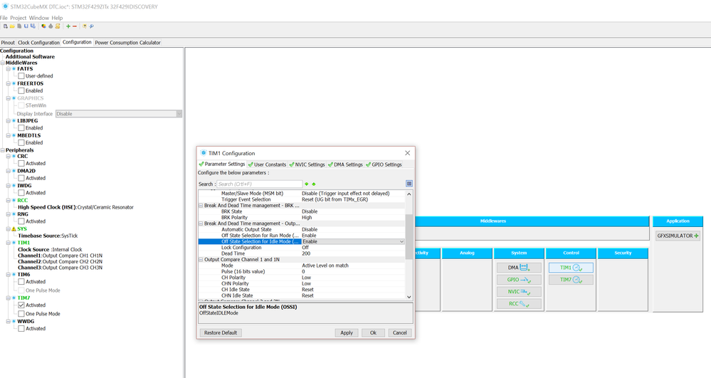
I'm trying to have complementary outputs with dead-time on CH1/CH2/CH3 and CH1/CH2/CH3N using TIM1 and Output Compare Mode on STM32F429.
So I configured STM32CubeMX like in the picture below :
And there is the portion of my code :
(for testing purposes, a button press changes the state of CH1/CH1N)
void TIM1_ItUpFcn()
{
		if (HAL_GPIO_ReadPin(GPIOA,GPIO_PIN_0)==1)
		{
			TIM1->CCER = 4;
		}
		else
			{
			TIM1->CCER = 5;
			}
}
That code changes CC1E/CC1NE bits.
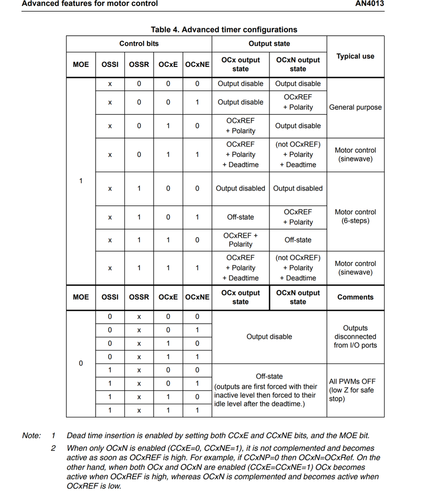
As a result,on the scope, I do get my complementary outputs on CH1 and CH1N, they invert each other when I press the button, but with no deadtime! I don't understand why i don't have that deadtime, like explained below :
Solved! Go to Solution.
Accepted Solutions
- Mark as New
- Bookmark
- Subscribe
- Mute
- Subscribe to RSS Feed
- Permalink
- Email to a Friend
- Report Inappropriate Content
2018-08-13 9:41 AM
So you have both CH1 and CH1N enabled in CCER, and CH1 set to OC1M = 0b001 i.e. set to active when match.
After enabling the timer, you should then see only one edge, first a falling one on CH1N, and then a rising one on CH1, delayed by 320 timer cycles.
You maybe expect that there is dead time inserted when you manipulate the outputs through CCER - this is not the case; dead time is related to the OCxREF signal and that does not change when you change CCER; see the Complementary outputs and dead-time insertion chapter in RM.
JW
- Mark as New
- Bookmark
- Subscribe
- Mute
- Subscribe to RSS Feed
- Permalink
- Email to a Friend
- Report Inappropriate Content
2018-08-12 10:58 PM
Read out and check/post the content of all TIM registers (mainly BDTR)
JW
- Mark as New
- Bookmark
- Subscribe
- Mute
- Subscribe to RSS Feed
- Permalink
- Email to a Friend
- Report Inappropriate Content
2018-08-13 8:21 AM
Hello,
In debug mode, BDTR=0x0000ACC8 (1010 1100 1100 1000)
There is the TIM1+TIM7 init code :
void DTC_initialize(void)
{
  /* Registration code */

  /* initialize error status */
  rtmSetErrorStatus(DTC_M, (NULL));

  /* user code (Start function Body) */

  /*Store TIM7 data information and its handler */
  G_TIM_Data[G_NbTimConf] = &TIM7_DataLink;
  G_TIM_Handler[G_NbTimConf] = &htim7;
  G_NbTimConf++;                       /*Inc number of configured TIM */

  /*Store TIM information */
  TIM7_DataLink.TIM_Prescaler = 8999;
  TIM7_DataLink.TIM_APBClock = 90000000;
  TIM7_DataLink.TIM_ARR = 5000 - 1;
  TIM7_DataLink.TIM_Clock = 10000.0;
  TIM7_DataLink.TIM_Freq = 2.0;
  TIM7_DataLink.CH1_duty = 0.0;
  TIM7_DataLink.CH2_duty = 0.0;
  TIM7_DataLink.CH3_duty = 0.0;
  TIM7_DataLink.CH4_duty = 0.0;
  TIM7_DataLink.CH1_type = UNKNOWN;
  TIM7_DataLink.CH2_type = UNKNOWN;
  TIM7_DataLink.CH3_type = UNKNOWN;
  TIM7_DataLink.CH4_type = UNKNOWN;

  /* Interrupt vector initialization */
  TIM7_DataLink.ItUpFcn = NULL;
  TIM7_DataLink.ItTrgFcn = NULL;
  TIM7_DataLink.ItComFcn = NULL;
  TIM7_DataLink.ItBrkFcn = NULL;
  TIM7_DataLink.ItCcFcn = NULL;

  /* Auto-reload preload enable */
  SET_BIT((&htim7)->Instance->CR1, TIM_CR1_ARPE);

  /*Update register value with blocset value*/
  /*Prescaler*/
  __HAL_TIM_SET_PRESCALER(&htim7,TIM7_DataLink.TIM_Prescaler);

  /*Autoreload: ARR */
  __HAL_TIM_SetAutoreload(&htim7, 5000 - 1);

  /* Time Base start IT */
  HAL_TIM_Base_Start_IT(&htim7);

  /* Update interrupt function */
  TIM7_DataLink.ItUpFcn = TIM7_ItUpFcn;

  /* Start interrupt for Update event*/
  HAL_TIM_Base_Start_IT(&htim7);

  /*Store TIM1 data information and its handler */
  G_TIM_Data[G_NbTimConf] = &TIM1_DataLink;
  G_TIM_Handler[G_NbTimConf] = &htim1;
  G_NbTimConf++;                       /*Inc number of configured TIM */

  /*Store TIM information */
  TIM1_DataLink.TIM_Prescaler = 0;
  TIM1_DataLink.TIM_APBClock = 180000000;
  TIM1_DataLink.TIM_ARR = 3600 - 1;
  TIM1_DataLink.TIM_Clock = 1.8E+8;
  TIM1_DataLink.TIM_Freq = 50000.0;
  TIM1_DataLink.CH1_duty = 0.0;
  TIM1_DataLink.CH2_duty = 0.0;
  TIM1_DataLink.CH3_duty = 0.0;
  TIM1_DataLink.CH4_duty = 0.0;
  TIM1_DataLink.CH1_type = OUTPUT_COMP;
  TIM1_DataLink.CH2_type = OUTPUT_COMP;
  TIM1_DataLink.CH3_type = OUTPUT_COMP;
  TIM1_DataLink.CH4_type = UNKNOWN;

  /* Interrupt vector initialization */
  TIM1_DataLink.ItUpFcn = NULL;
  TIM1_DataLink.ItTrgFcn = NULL;
  TIM1_DataLink.ItComFcn = NULL;
  TIM1_DataLink.ItBrkFcn = NULL;
  TIM1_DataLink.ItCcFcn = NULL;

  /* Auto-reload preload enable */
  SET_BIT((&htim1)->Instance->CR1, TIM_CR1_ARPE);

  /*Update register value with blocset value*/
  /*Prescaler*/
  __HAL_TIM_SET_PRESCALER(&htim1,TIM1_DataLink.TIM_Prescaler);

  /*Autoreload: ARR */
  __HAL_TIM_SetAutoreload(&htim1, 3600 - 1);

  /*Set CH1 Pulse value*/
  __HAL_TIM_SetCompare(&htim1, TIM_CHANNEL_1, (uint32_t)((3600 - 1)/2));

  /*Set CH2 Pulse value*/
  __HAL_TIM_SetCompare(&htim1, TIM_CHANNEL_2, (uint32_t)((3600 - 1)/2));

  /*Set CH3 Pulse value*/
  __HAL_TIM_SetCompare(&htim1, TIM_CHANNEL_3, (uint32_t)((3600 - 1)/2));

  /* Wait for htim1 State READY */
  while ((&htim1)->State == HAL_TIM_STATE_BUSY) {
  }

  HAL_TIM_OC_Start(&htim1, TIM_CHANNEL_1);

  /* Enable the complementary OC output 1 */
  HAL_TIMEx_OCN_Start(&htim1, TIM_CHANNEL_1);

  /* Wait for htim1 State READY */
  while ((&htim1)->State == HAL_TIM_STATE_BUSY) {
  }

  HAL_TIM_OC_Start(&htim1, TIM_CHANNEL_2);

  /* Enable the complementary OC output 2 */
  HAL_TIMEx_OCN_Start(&htim1, TIM_CHANNEL_2);

  /* Wait for htim1 State READY */
  while ((&htim1)->State == HAL_TIM_STATE_BUSY) {
  }

  HAL_TIM_OC_Start(&htim1, TIM_CHANNEL_3);

  /* Enable the complementary OC output 3 */
  HAL_TIMEx_OCN_Start(&htim1, TIM_CHANNEL_3);

  /* Update interrupt function */
  TIM1_DataLink.ItUpFcn = TIM1_ItUpFcn;

  /* Start interrupt for Update event*/
  HAL_TIM_Base_Start_IT(&htim1);
  ;
  ;
  ;
  ;
}- Mark as New
- Bookmark
- Subscribe
- Mute
- Subscribe to RSS Feed
- Permalink
- Email to a Friend
- Report Inappropriate Content
2018-08-13 9:02 AM
And the rest of the registers? I don't Cube.
JW
- Mark as New
- Bookmark
- Subscribe
- Mute
- Subscribe to RSS Feed
- Permalink
- Email to a Friend
- Report Inappropriate Content
2018-08-13 9:12 AM
- Mark as New
- Bookmark
- Subscribe
- Mute
- Subscribe to RSS Feed
- Permalink
- Email to a Friend
- Report Inappropriate Content
2018-08-13 9:41 AM
So you have both CH1 and CH1N enabled in CCER, and CH1 set to OC1M = 0b001 i.e. set to active when match.
After enabling the timer, you should then see only one edge, first a falling one on CH1N, and then a rising one on CH1, delayed by 320 timer cycles.
You maybe expect that there is dead time inserted when you manipulate the outputs through CCER - this is not the case; dead time is related to the OCxREF signal and that does not change when you change CCER; see the Complementary outputs and dead-time insertion chapter in RM.
JW
- Mark as New
- Bookmark
- Subscribe
- Mute
- Subscribe to RSS Feed
- Permalink
- Email to a Friend
- Report Inappropriate Content
2018-08-14 1:27 AM
Okay, so I finally found how to turn ON CH1/CH2/CH3 and CH1/CH2/CH3N with the appropriate deadtime, using CCMR1 and CCMR2 registers (by setting bits 4-6 for OC1M, bits 12-14 for OC2M on CCMR1, bits 4-6 for OC3M on CCMR2).
- HRTIM PWM transients greater than a period in STM32 MCUs Products
- Improvement needed (manual) - G431 in STM32 MCUs Products
- Proper output config for complementary HRTIM outputs in STM32 MCUs Embedded software
- Cannot set deadtime for HRTIM1 in NUCLEO-G474 in STM32 MCUs Products
- STM32G431 + DRV8323H - High-side FETs overlapping despite hardware dead time in STM32 MCUs Motor control

